PCB Capabilities
PCB Manufacturing Capabilities
PCBELEC provides PCB manufacturing capabilities for a wide range of rigid, flexible, rigid-flex, HDI, multilayer, heavy copper, and controlled impedance projects. This page gives engineers, buyers, and sourcing teams a structured overview of our fabrication range, process limits, advanced build options, supported materials, surface finishes, and testing resources before moving into a dedicated capability page or requesting a quotation.
PCB Capability Overview
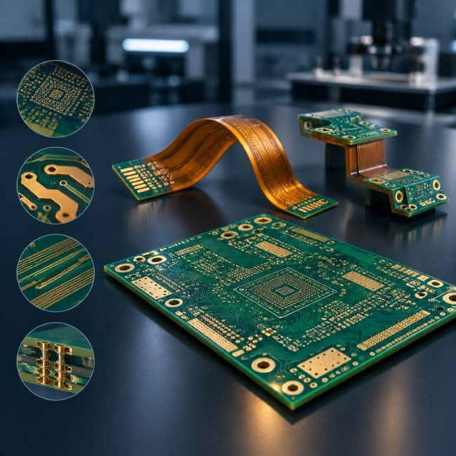
PCBELEC supports PCB fabrication across both standard and advanced build categories, including multilayer rigid PCBs, flexible circuits, rigid-flex boards, HDI structures, heavy copper designs, controlled impedance boards, and selected high-speed or high-frequency constructions. Our manufacturing capability is not limited to basic board fabrication; it also includes the process controls that matter in real projects, such as trace and spacing capability, drilling limits, copper balancing, finish selection, mechanical processing, and electrical verification.
From standard multilayer fabrication to more advanced structures, the capability scope covers the process areas most often reviewed in real PCB projects, including materials, drilling, surface finish, testing, HDI, rigid-flex, and other fabrication-sensitive requirements. More detailed capability information for specific structures is available in the dedicated pages for rigid PCB, flexible PCB, rigid-flex PCB, HDI PCB, stencil fabrication, and other specialized manufacturing categories.
Capability Snapshot
The snapshot below highlights the most frequently reviewed PCB manufacturing parameters during supplier evaluation and early-stage engineering review. These are summary values intended for quick reference; advanced or application-sensitive builds should be confirmed with stackup data and project files.
Layer Count
Up to 30 layers in the standard capability overview, with higher-complexity builds reviewed according to stackup, thickness, and application requirements.
Board Thickness
Finished board thickness capability from 0.1 mm to 8.0 mm depending on structure, board type, and order profile.
Copper Weight
Outer layer finished copper up to 8 oz and inner layer finished copper up to 6 oz for suitable projects.
Fine Line
Inner-layer fine line capability down to 2/2 mil, with geometry limits varying by copper thickness and structure.
Mechanical Drill
Mechanical drill capability down to 0.15 mm for applicable designs.
Laser Via / HDI
Standard laser via capability down to 4 mil, with smaller microvia structures available after engineering review.
Impedance Control
Controlled impedance support for selected stackups and signal-critical designs.
Surface Finishes
Support for ENIG, ENEPIG, OSP, HASL, lead-free HASL, immersion tin, immersion silver, hard gold, and related finish options.
Core PCB Manufacturing Capabilities
Our core manufacturing capabilities cover the process parameters most frequently used during PCB sourcing, engineering review, and supplier qualification. The table below summarizes the practical manufacturing range for board types, layers, copper weight, line and spacing, drilling, materials, surface finishes, profiling, and test support.
Use this table as a structured overview of general capability. For advanced HDI, special materials, high-speed designs, backdrilling, or complex via structures, please refer to the advanced capability section below or submit your files for engineering review.
| Category | Capability | Typical Range / Support | Notes |
|---|---|---|---|
| Board Types | Supported PCB structures | Rigid PCB, Flexible PCB, Rigid-Flex PCB, HDI PCB, Heavy Copper PCB, Controlled Impedance PCB, Blind/Buried Via PCB, Backdrill PCB, Gold Finger PCB | Special structures are reviewed according to stackup, copper balance, drilling, and end-use requirements. |
| Layer Count | Maximum layer capability | Up to 30 layers | Higher-layer or high-complexity builds should be reviewed by engineering before quotation. |
| Board Thickness | Finished board thickness | 0.1 mm – 8.0 mm | Available range depends on board type, structure, and order profile. |
| Copper Weight | Finished copper weight | Outer layer up to 8 oz; inner layer up to 6 oz | Heavy copper designs should be evaluated together with trace width, spacing, and thermal requirements. |
| Fine Line | Minimum inner-layer trace / spacing | Down to 2/2 mil | Actual capability depends on copper thickness, layer position, and structure type. |
| Mechanical Drill | Minimum mechanical drill size | Down to 0.15 mm | Final support depends on board thickness, hole count, aspect ratio, and annular ring design. |
| Laser Via / HDI | Laser via capability | Standard down to 4 mil | More advanced microvia structures are available for suitable HDI projects after engineering review. |
| Via Structures | Supported via types | Through hole, blind via, buried via, via filling, stacked / staggered HDI structures | Availability depends on buildup design, lamination sequence, and reliability requirements. |
| Aspect Ratio | Hole aspect ratio support | Based on structure and process route | Advanced aspect ratios should be reviewed case by case for manufacturability and reliability. |
| Impedance Control | Controlled impedance fabrication | Supported for selected stackups and target structures | Tolerance depends on target impedance, material system, copper distribution, and layer structure. |
| Materials | Supported material systems | Standard FR4, High Tg, Halogen-Free, High CTI, High-Speed / Low-Loss, High-Frequency, Aluminum-backed, Flex and Rigid-Flex materials | Material selection should follow electrical, thermal, mechanical, and reliability requirements. |
| Surface Finishes | Available finish options | HASL, Lead-Free HASL, ENIG, ENEPIG, OSP, Immersion Tin, Immersion Silver, Hard Gold, Gold Fingers, Selective Gold | Finish choice depends on solderability, bonding, wear resistance, storage, and application environment. |
| Profiling | Board outline and mechanical processing | Routing, V-cut, Punch, Beveling, Selected depth-control processing | Mechanical tolerances depend on board thickness, outline complexity, and panel design. |
| Solder Mask & Legend | Mask and marking capability | Standard and custom solder mask options with legend printing support | Fine legend and mask clearance capability depends on copper layout and finished board design. |
| Testing | Electrical and process verification | E-test, Flying Probe, Cross-section, Microscope Inspection, Impedance Test, High-Pot | Test strategy depends on product type, netlist availability, layer count, and final application. |
| Reliability Support | Additional reliability-related verification | Tg Test, Peel Strength, Ionic Testing, IR Reflow, Thermal Chamber and related evaluations | Available reliability checks vary by product type and project requirement. |
Advanced PCB Capabilities
Some PCB projects go beyond standard multilayer fabrication and require additional engineering review before final manufacturability can be confirmed. These include advanced HDI structures, microvias, blind and buried vias, repeated lamination, backdrilling, low-loss or RF materials, heavy copper builds, and other structure-sensitive designs where stackup, dielectric thickness, copper distribution, and reliability targets all affect the process route.
The advanced capability table below is intended to show what types of higher-complexity projects can be supported and which areas typically require tighter engineering coordination.
| Advanced Area | Capability | Typical Support | Engineering Notes |
|---|---|---|---|
| HDI Structures | HDI construction support | Laser-via HDI, blind/buried via builds, stacked or staggered buildup structures | Structure selection depends on buildup count, dielectric thickness, via target, copper balance, and reliability requirements. |
| Laser Via | Laser microvia capability | Standard down to 4 mil; 3 mil available for selected structures subject to review | Smaller microvia capability depends on dielectric type, PP structure, and buildup design. |
| HDI Build-up | Laser build-up stages | Prototype capability up to 5-stage laser build-up; production-oriented structures reviewed by project | Higher build-up counts should be confirmed with lamination sequence, reliability target, and end application. |
| Blind / Buried Vias | Advanced via structures | Blind via, buried via, via fill, and mixed multilayer interconnect structures | Via reliability, fill quality, and registration must be reviewed together with final stackup. |
| Sequential Lamination | Multi-lamination support | Repeated lamination on the same core up to 5 cycles in reviewed structures | Projects above standard lamination complexity require engineering review before quotation. |
| Backdrilling | Backdrill capability | Backdrill support for signal integrity and high-speed designs; minimum backdrill hole diameter from 0.15 mm for plated holes | Target layer spacing, residual stub limits, and dielectric thickness must be evaluated before fabrication release. |
| Backdrill Accuracy | Backdrill depth tolerance | Prototype ±0.02 mm; production ±0.03 mm | Best suited to high-speed, backplane, and mixed high-frequency structures requiring stub control. |
| High-Speed Materials | Low-loss / high-speed laminate support | Material systems for 1–5G, 5–10G, 10–25G, and above-25G classes depending on stackup and sourcing route | Final material recommendation depends on loss budget, target data rate, layer structure, and fabrication compatibility. |
| High-Frequency Materials | RF and microwave material support | Selected Rogers, Taconic, Arlon and related ceramic-filled or PTFE-based systems | PTFE or mixed high-frequency builds may require mechanical blind/buried drilling, controlled-depth processing, or special lamination review. |
| Hybrid Constructions | Mixed material stackups | High-speed, high-frequency, ceramic-filled, PTFE, and hybrid rigid constructions for selected applications | Not all mixed-material structures are suitable for standard HDI laser routing or direct copper-foil lamination. |
| Fine Pitch / BGA | Fine-pitch routing support | Advanced BGA fan-out and fine-line routing available for suitable pad and finish structures | Capability depends on pad diameter, finish type, solder mask design, and final line/space requirement. |
| Hole-to-Copper Control | Tight clearance structures | Reduced drill-to-copper and laser-via-to-conductor spacing available for reviewed structures | Clearance feasibility depends on layer count, via type, resin flow, registration, and reliability margin. |
| Special Hole Structures | Complex mechanical hole features | Stepped holes, tapered holes, controlled-depth slots, plated and non-plated slot processing | Hole angle, depth tolerance, diameter tolerance, and slot geometry should be reviewed with the mechanical drawing. |
| Special Surface Finish | Advanced finish combinations | ENEPIG, selective gold, hard gold, gold fingers, ENIG + OSP, and other finish combinations for selected applications | Finish compatibility should be matched to bonding, wear resistance, solderability, and storage requirements. |
| Heavy Copper Builds | High-copper advanced structures | Heavy copper routing and multilayer constructions with copper-dependent line control | Trace width, spacing, plating uniformity, thermal balance, and resin flow should be reviewed in advance. |
| Reliability-Oriented Projects | Advanced process verification support | Cross-section, impedance verification, high-pot, ionic testing, Tg test, peel strength, IR reflow, thermal chamber and related checks | Verification plan should be defined according to application environment, qualification target, and project risk level. |
Supported Materials and Laminate Systems
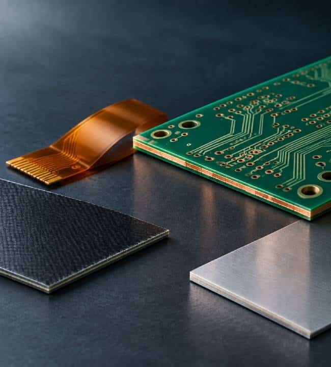
Material selection plays a central role in PCB performance, manufacturability, and reliability. PCBELEC supports standard FR4 constructions as well as selected high Tg, halogen-free, high CTI, high-speed, low-loss, high-frequency, aluminum-backed, and flex-compatible material systems, depending on project type and fabrication route.
For advanced projects, material choice should be evaluated together with electrical targets, thermal load, bend requirements, dielectric thickness, copper balance, and final application conditions. In many cases, the best-performing material is not simply the highest-grade laminate, but the one that best matches the structure, signal requirement, and production route.
- Standard FR4 and lead-free compatible FR4
- High Tg materials
- Halogen-free and high CTI materials
- High-speed / low-loss materials
- High-frequency / RF materials
- Flex and rigid-flex material systems
Surface Finishes and Coating Options
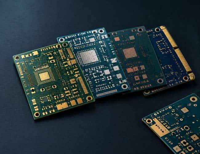
Surface finish affects solderability, oxidation resistance, bonding compatibility, wear resistance, storage life, and final-use reliability. PCBELEC supports a broad range of finish options for different PCB manufacturing requirements, including mainstream assembly-oriented finishes, precious-metal finishes, and selected finish combinations for specialized applications.
Available finish options include HASL, lead-free HASL, ENIG, ENEPIG, OSP, immersion tin, immersion silver, hard gold, gold fingers, and selective gold. The most suitable finish depends on your soldering process, connector wear requirements, bonding needs, storage conditions, and target cost balance.
Equipment and Process Control
Manufacturing capability is not defined by parameter sheets alone. It also depends on process stability, equipment control, inspection discipline, and the factory’s ability to repeat critical steps across engineering, imaging, drilling, plating, finishing, and final verification.
Our process resources include CAM and plotting systems, AOI platforms, vacuum lamination presses, mechanical drilling and laser drilling equipment, LDI exposure, automatic plating lines, via-fill processes, solder mask coating systems, legend printing, routing and V-cut equipment, and multiple test and reliability evaluation resources. These capabilities support better process control across both standard and advanced PCB fabrication projects.
- Engineering & CAM: Frontline InPlan, Genesis 2000, photo plotting systems
- Imaging & AOI: Orbotech, Camtek, LDI exposure resources
- Drilling: Hitachi, Schmoll, Mitsubishi drilling systems and laser drill support
- Plating: pattern plating, panel plating, and via-fill related capability
- Surface finish: Uyemura ENIG / ENEPIG, OSP, immersion processes, gold-related finishes
- Test & reliability: E-test, flying probe, X-section, impedance test, high-pot, Tg test, peel strength, ionic testing, IR reflow, thermal chamber
Explore Capability by PCB Type
If you need more detailed information for a specific board category, explore the dedicated capability pages below. Each page focuses on the manufacturing considerations, structure limits, and practical review points for that PCB type.
Rigid PCB Fabrication Capability
Explore multilayer rigid PCB capability across layer count, copper weight, drilling, line control, finishes, and structural tolerances for standard and advanced rigid board projects.
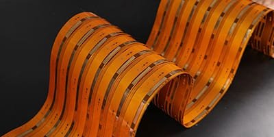
Flexible PCB Fabrication Capability
Review flexible PCB capability for material, coverlay, stiffener, bend-sensitive structures, and fabrication requirements for static or dynamic flex applications.
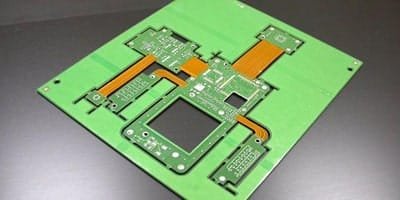
Rigid-Flex PCB Fabrication Capability
Understand rigid-flex capability for mixed stackups, flex-to-rigid transitions, via design constraints, and fabrication review points for higher-reliability structures.
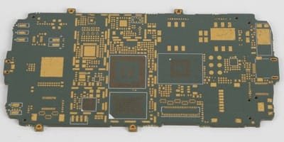
HDI PCB Board Fabrication Capability
Check HDI capability for laser vias, buildup layers, blind and buried vias, finer geometry, tighter registration, and density-driven designs.
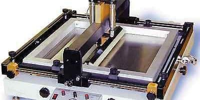
PCB SMT Stencil Fabrication Capabilities
View stencil-related capability for thickness selection, aperture precision, fine-pitch requirements, and support for accurate solder paste deposition planning.

PCB Copper Thickness Capabilities
Compare standard and heavy copper capability for power boards, thermal designs, thick-copper routing, and copper-weight-dependent trace and spacing constraints.
Frequently Asked Questions About PCB Manufacturing Capabilities
PCBELEC supports a wide multilayer range, with standard overview capability up to 30 layers and engineering review for higher-complexity structures. Final support depends on stackup design, thickness, copper requirement, via construction, and application needs.
For suitable builds, inner-layer fine line capability can reach 2/2 mil. The actual manufacturable value depends on copper thickness, layer position, structure type, and yield risk.
Yes. HDI-related manufacturing support includes laser vias, blind and buried vias, build-up structures, and fine-feature routing for suitable projects.
PCBELEC supports both standard and heavy copper constructions, with outer-layer finished copper up to 8 oz and inner-layer finished copper up to 6 oz for applicable projects.
Available finishes include HASL, lead-free HASL, ENIG, ENEPIG, immersion tin, immersion silver, OSP, hard gold, gold fingers, and selective gold, depending on the board structure and end-use requirement.
Yes. Controlled impedance support is available for selected stackups and target structures, with tolerance performance influenced by materials, copper distribution, layer geometry, and target impedance values.
Yes. The capability scope includes both flex and rigid-flex PCB fabrication, with engineering review focused on material type, bend area design, stiffeners, stackup transition, and structural complexity.
Engineering review is strongly recommended for advanced HDI, high layer count, special materials, unusual copper distribution, tight hole-to-copper structures, backdrilling, and other designs that go beyond standard fabrication ranges.
Request a PCB Capability Review
If your project involves special materials, HDI structures, high layer counts, heavy copper, controlled impedance, backdrilling, or other fabrication-sensitive requirements, send us your Gerber files, stackup, material preferences, copper weight, finish requirements, and target specifications for engineering review. Our team can evaluate manufacturability and guide you toward a suitable fabrication route before quotation.