Table of Contents
Why Panelization Matters for Gold Finger PCBs
Gold finger PCBs are already more demanding than standard boards in terms of design rules, plating, and inspection, and panelization adds another layer of complexity on top. The way you arrange boards on a panel, orient the gold finger edges, and place routing and break‑off tabs directly affects plating uniformity, bevel quality, depanelization stress, and ultimately the yield and reliability of your edge connectors.
Many common problems—scratched contacts, uneven bevels, exposed copper at the edge, or cracked fingers after depanelization—can be traced back to panel and routing decisions rather than to the connector footprint itself. This article focuses on practical panelization and routing strategies specifically for gold finger PCBs, so you can get more good boards per panel while keeping the connector area robust enough for real‑world use. If you are planning a new design, you can cross‑check these guidelines against our “Gold Finger PCB Fabrication & Manufacturing Service” to ensure your panel layout matches real manufacturing capabilities.
Key Panelization Principles for Gold Finger Boards
Before diving into specific orientations and routing patterns, it helps to define a few overarching principles that should guide any gold finger panel design. These principles will influence how you place boards, choose depanelization methods, and define keep‑outs around the connector edge.
1. Keep gold fingers on a consistent panel edge
For reliable plating and beveling, gold finger edges should be aligned along a consistent side of the panel rather than pointing in different directions. This allows the manufacturer to run the panel through plating, beveling, and inspection steps with predictable tooling and fixturing, improving both yield and repeatability.
Whenever possible, place the gold finger edge on the outer perimeter of the panel instead of burying it in the interior between other boards. This provides easier access for plating buses, bevel tools, and inspectors, and reduces the chance that routing paths or tabs will interfere with the connector area.
2. Separate connector edges from aggressive depanelization features
Depanelization always introduces mechanical stress, and if that stress is concentrated near the gold fingers, it can damage plating or the laminate around the connector. A core principle is to keep V‑grooves, large mouse‑bites, and break‑off tabs away from the finger edge and focus them on non‑critical sides of the board wherever the outline allows.
If the design forces you to place tabs near the connector side, make them as small and few as possible and ensure that routers or punches will not scuff the beveled edge during separation. You can then reinforce handling guidelines so operators support the board properly when snapping or cutting panels apart.
3. Maintain adequate clearance around the finger region
Panelization does not remove the need for local keep‑outs around the gold finger area. You still need a clear zone free of vias, copper pours, test pads, and large mechanical features, and this keep‑out must be respected at both the individual‑board level and the panel level.
On the panel drawing, avoid putting tooling holes, fiducials, or rail‑mounted components too close to the gold finger edge. This preserves space for beveling and finishing tools and reduces the risk that panel fixtures will contact or scratch the plated connectors.
4. Align with standard panel sizes and methods
Good gold finger panelization also means making efficient use of standard panel sizes and depanelization methods (V‑scoring, tab‑routing, or hybrids). Aligning your board outline and connector edge with these standard options usually allows more boards per panel and more predictable depanelization behavior.
If you find yourself needing unusual panel sizes, many tiny boards with gold fingers, or complex mixed methods, it is worth involving your PCB manufacturer early. They can often suggest small changes to outline, connector orientation, or rail design that improve panel utilization and reduce the risk of damage to the connector edge.
Orienting Gold Fingers on the Panel for Consistent Plating and Beveling
Getting the orientation of gold fingers right at the panel level is essential for consistent plating thickness, bevel quality, and connector performance. If boards are rotated randomly or the connector edge is buried inside the panel, it becomes much harder for the fabricator to control processes and inspect results.
1. Align all gold finger edges in a common direction
The first rule is simple: keep all gold finger edges pointing in the same direction on the panel. This allows the panel to move through plating and beveling machines with a single, consistent reference edge, so tooling, clamps, and bevel cutters can be optimized for that side.
In practice, that means rotating individual board images in your panel drawing so the connector edges line up along a common panel side instead of alternating or facing inward. If you are unsure which edge is best, you can confirm the preferred orientation with your manufacturer up front, or use their “Gold Finger PCB Fabrication & Manufacturing Service” guidelines as a reference.
2. Put the connector edge on the panel perimeter when possible
Whenever the outline permits, place the gold finger edge directly on the outer perimeter of the panel rather than between rows of boards. A perimeter location gives beveling tools and inspectors direct access to the connector without routing in between boards, which lowers the risk of accidental scuffs or mis‑aligned chamfers.
Some manufacturers also require a minimum length along the panel edge for proper beveling—commonly on the order of 30 mm or more—so that the board can be held securely and the cut can be made cleanly. Very narrow modules may need extra rails or special handling to meet these constraints, so it is worth checking your outline against typical beveling requirements early in the design.
3. Reserve bevel clearance between fingers and final edge
Beveling removes material at an angle, so the distance between the gold finger pads and the final board edge must be sufficient to avoid cutting into the plated contacts. Guidelines from multiple manufacturers suggest keeping at least about 0.6–1.0 mm between the end of the finger pads and the edge that will be beveled, depending on board thickness and the chosen angle.
When you create your panel outline, make sure routing paths and any pre‑routing to separate boards do not reduce this clearance. If the bevel depth plus manufacturing tolerances could potentially reach into the plated area, adjust either the pad‑to‑edge distance or the bevel specification before releasing the design.
4. Match bevel angle and depth to connector and process
Common bevel angles for gold fingers are 30° and 45°, with 30° widely used as a good balance between insertion ease and remaining contact area. Your fabrication notes should explicitly state the desired bevel angle and whether it applies to one or both sides of the board edge, rather than leaving it as an implied default.
At the panel level, this bevel specification affects how much material is removed and how close adjacent boards or rails can be placed to the connector side. If your mating connector or mechanical envelope demands a non‑standard bevel, it is especially important to confirm feasibility with your PCB house—ideally by sharing your panel drawing and requirements through their Gold Finger PCB manufacturing support channel before locking the design.
Routing, Tabs, and Break‑off Features Near the Gold Finger Edge
How you route panels and design break‑off features around the connector side has a direct impact on both yield and long‑term connector reliability. Poorly placed tabs, aggressive V‑scores, or tight routing paths can crack laminate, chip the bevel, or leave rough edges that damage the mating connector over time.
1. Prefer non‑connector edges for tabs and mouse bites
As a general rule, place tab‑routing bridges and mouse‑bite perforations on edges away from the gold fingers whenever the outline allows. This keeps the highest depanelization stress away from the connector, so any micro‑cracks or roughness that occur at the break line will not affect the plated contact area.
When gold fingers must be on a short side and there are few other edges available, concentrate tabs near mechanically robust regions—such as corners with plenty of laminate and no dense traces—rather than near the finger cluster itself. In your panel drawing, you can explicitly mark the connector edge as a “no‑tab zone” so CAM engineers do not add break‑off features there during optimization.
2. Control tab size, count, and placement
For tab‑routed panels, each tab should be just strong enough to support the board during assembly, but not so wide or numerous that excessive force is needed to separate the panel. A typical mouse‑bite tab might use 5–7 small holes (around 0.3–0.5 mm) across a 1–2 mm width, spaced so that the fracture path is well controlled.
Keep tabs at least a couple of millimeters away from sensitive traces, plated holes, and any copper features that could crack under depanelization stress. For gold finger PCBs, that “sensitive zone” includes the connector edge itself and any nearby routing that supports the fingers mechanically, so plan your tabs accordingly at the panel level.
3. Use V‑scoring carefully near edge connectors
V‑scoring is efficient for rectangular boards, but it introduces a continuous line of weakened material that can concentrate stress along the entire edge. When that edge also contains gold fingers, an overly deep or misaligned V‑groove can cause chipping or minor fractures close to the plated contacts.
If you must V‑score on a side that includes gold fingers, coordinate score depth and position with your manufacturer and maintain extra clearance between the score line and the start of the fingers. In many cases, a hybrid approach—tab‑routing near the connector side and V‑scoring on other edges—provides a better balance between panel stiffness and depanelization stress.
4. Keep routing tools away from the beveled edge
Mechanical routing paths should never run so close to the connector edge that the router bit risks grazing the bevel or leaving burrs in the plated area. Define a clear keep‑out band for routing around the gold finger edge at the panel level, taking into account tool diameter and any manufacturing tolerances.
If your board shape forces routed profiles near the connector, discuss minimum tool‑to‑finger distance and preferred routing order with your PCB house. Many manufacturers can suggest small outline changes or rail extensions that move routing operations slightly away from the critical edge, and you can validate those suggestions against your connector and mechanical constraints using their Gold Finger PCB fabrication guidelines.
5. Plan for post‑depaneling edge finishing where needed
Even with carefully designed tabs and routing, some panelization schemes will leave small nibs or roughness at break points. When these are near areas that slide against metal guides or connector housings, light sanding or secondary edge finishing may be required to avoid mechanical wear over time.
If your product has tight mechanical constraints or high insertion counts, it can be worth specifying a basic post‑depaneling edge‑finish requirement in your build notes. For complex gold finger assemblies, you can also consult your manufacturer through their “Gold Finger PCB Fabrication & Manufacturing Service” channel to see what level of edge finishing they can provide as part of the standard process versus an optional upgrade.
Fiducials, Registration, and Keep‑Outs for Reliable Connectors
Accurate registration is especially important for gold finger PCBs because small misalignments can shift bevels, routing paths, or solder mask openings relative to the connector edge. Good fiducial placement and clearly defined keep‑outs help your manufacturer hold tight tolerances where the edge connector matters most.
1. Use global panel fiducials to stabilize the whole array
Global fiducials on the panel rails give assembly and fabrication equipment a stable reference for the entire array. A common best practice is to place three global fiducials in an L‑shape on the panel frame—typically near three corners—so machines can correct for rotation, scale, and slight warpage.
Keep a clear area around each fiducial (usually 1–2 mm free of copper, mask openings, or text) to ensure camera systems can detect them reliably. Avoid placing fiducials on or near V‑score lines, break‑off tabs, or routed edges, because mechanical stress and chipping in those areas can degrade the mark over time.
2. Add local fiducials near critical connector features when needed
For boards with very fine‑pitch components or tight connector tolerances, local fiducials on the individual PCB can improve registration for both assembly and any connector‑related processing. Place at least two local fiducials diagonally around critical zones such as high‑density connectors or edge‑connector regions that must line up precisely with housings or guides.
As with global fiducials, maintain a small keep‑out area around each local mark and ensure they are implemented as exposed copper pads without solder mask. If your design is tight on space, your PCB house can advise whether global panel fiducials alone are sufficient, or whether local fiducials near the gold finger region will meaningfully improve alignment.
3. Define strict keep‑out zones around gold fingers
Gold fingers need a clean zone free of interfering features so that plating, beveling, and connector mating are not obstructed. Typical keep‑out rules include prohibiting plated through‑holes, vias, test pads, and silkscreen within a certain distance (for example 1–2 mm) from the finger base and along the edge where beveling occurs.
These keep‑outs should be defined both in the PCB layout and on the panel drawing, so that panel‑level features like tooling holes, fiducials, and tabs are also kept away from the connector edge. Neglecting panel‑level keep‑outs can lead to situations where a perfectly designed board is compromised by a tooling hole or tab placed too close to the beveled fingers.
4. Coordinate keep‑outs with stack‑up and inner‑layer copper
Keep‑out planning is not limited to the outer layers. Removing or pulling back inner‑layer copper under the gold finger region prevents “telegraphing” of internal planes during beveling and reduces the chance of exposed copper at the edge.
Your stack‑up definition should therefore include explicit copper pull‑backs near the connector, coordinated with the bevel depth and edge tolerances. Many manufacturers include recommended values for these pull‑backs in their Gold Finger PCB fabrication design notes, and you can verify your DRC rules against those before releasing Gerbers.
5. Document registration and keep‑out expectations in your fab notes
Finally, make your expectations explicit in the fabrication drawing and panel documentation. Call out the presence and purpose of global and any local fiducials, define no‑go areas near the gold fingers for tabs, tooling holes, and routing, and reference any specific tolerances that are critical for the edge connector.
Sharing this information early—ideally when you first submit your design through a “Gold Finger PCB Fabrication & Manufacturing Service” request—helps your PCB partner align their CAM setup and panelization strategy with your reliability goals. It also reduces back‑and‑forth during quoting and DFM, shortening the path from design to stable production panels.
High‑Speed and Power Routing into Gold Fingers
Gold fingers are not just mechanical contacts; for many designs they carry high‑speed interfaces and significant power, so how you route into the connector region matters as much as the panelization itself. Good routing around the edge connector reduces reflections, crosstalk, and localized heating, and makes the whole assembly more tolerant of manufacturing variation.
1. Keep high‑speed paths short and direct
For high‑speed signals, minimize the distance between the gold finger and the first active device or termination network. Short, direct routes reduce insertion loss and make it easier to maintain impedance control through the transition into the connector.
Avoid unnecessary via transitions in the short segment between the device and the finger whenever possible. If vias are unavoidable, use back‑drilling or via‑stubs reduction techniques and keep the via count low in the edge‑connector escape region.
2. Maintain impedance and reference planes up to the edge
Treat gold finger traces as part of your controlled‑impedance channel. That means keeping a solid reference plane under the finger traces (usually ground) and maintaining consistent trace width and spacing as they approach the edge.
For differential pairs, route the pair all the way into the fingers with matched length and spacing and avoid sudden neck‑downs or asymmetrical fan‑outs right before the connector. When stack‑up or panel constraints force changes in reference plane or geometry, simulate or at least calculate impedance for the edge region so you understand the impact.
3. Control spacing and crosstalk between fingers
High‑speed edge connectors pack many signals into a small space, so crosstalk can become a problem if fingers are too close or poorly grouped. Where the connector specification allows, maintain at least several times the trace width as spacing between unrelated high‑speed lines and consider inserting ground fingers or reserved gaps between especially sensitive pairs.
Group fingers logically—keep differential pairs adjacent and balanced, cluster noisy signals away from very sensitive lines, and avoid mixing very fast edges right next to analog or low‑jitter clock signals on the connector. These decisions are best made early in the pin‑assignment stage, not as late fixes in the layout.
4. Design power fingers for current and sequencing
Power fingers should be sized and routed according to their current and sequencing requirements. Use wider pads and thicker copper for high‑current rails, and minimize neck‑downs and sharp corners in the short path from the power plane to the finger.
If your system relies on make‑before‑break or staggered power sequencing, use stepped or offset finger lengths as recommended by the connector vendor and ensure panelization and beveling preserve those length differences accurately. Document any special sequencing requirements in your fab and assembly notes so the connector, gold finger geometry, and manufacturing flow all support the intended behavior.
5. Respect keep‑outs and avoid last‑minute “squeezing” of traces
When panel or mechanical constraints become tight, there is a temptation to “squeeze” extra traces through the edge‑connector region, but this often violates keep‑outs or compromises impedance. It is better to revisit the connector pin‑out or overall board outline than to add extra vias, sharp jogs, or very narrow trace neck‑downs right before the fingers.
Before releasing Gerbers, run a focused DRC around the connector area with stricter rules for minimum spacing, trace width, and copper‑to‑edge clearance. If you are unsure whether your current routing into the gold fingers is manufacturable or robust enough, you can include this region as a specific checkpoint when you submit files through a “Gold Finger PCB Fabrication & Manufacturing Service” DFM review request.
Common Panelization Mistakes That Hurt Yield
Even when the connector footprint and routing look perfect, a few recurring panelization mistakes can quietly reduce yield or damage gold fingers during manufacturing and depanelization. Being aware of these pitfalls makes it easier to spot them early in DFM and correct them before they show up as scrap on the line.
1. Random board orientation and mixed connector edges
One of the most common issues is rotating boards arbitrarily on the panel so that gold finger edges face different directions. This forces the factory to either use sub‑optimal tooling or run multiple setups for plating and beveling, which increases variation and the chance of uneven bevels, tool marks, or mis‑alignment.
The fix is to standardize orientation: choose one panel edge for all gold fingers and keep it consistent across the array. This not only improves quality but also makes it easier for your fabricator to apply their standard Gold Finger PCB panelization process.
2. Tabs or V‑scores too close to the gold finger edge
Placing mouse‑bite tabs or V‑score lines close to the edge connector concentrates depanelization stress in the most sensitive region of the board. The result can be chipped bevels, micro‑cracks in the laminate, or rough edges that interfere with smooth insertion.
Design guidelines recommend keeping break‑off features away from connector edges and using routing or tabs on non‑critical sides whenever possible. If the outline forces you to share an edge, you may need smaller, fewer tabs and carefully tuned V‑score depth to control the fracture path and limit edge damage.
3. Insufficient clearance between routing paths and connector edges
Another frequent mistake is running panel‑level routing too close to the gold finger edge. When the router bit passes near the connector, even small deviations in tool path or board position can leave burrs or nick the bevel, especially on thicker panels or when tools are worn.
The better practice is to define a routing keep‑out band around the connector edge that accounts for tool diameter, tolerances, and any required bevel depth. If this is difficult to achieve given your current outline, it is often cheaper to adjust the board shape or add rails than to accept a higher risk of edge damage.
4. Ignoring manufacturer panel size and process limits
Designers sometimes create panels that look efficient on screen but do not fit well within the manufacturer’s standard panel sizes or plating line constraints. Panels that are too large, too dense, or shaped awkwardly can suffer from uneven plating, warpage, or poor edge quality after machining.
Consulting your PCB fab’s recommended panel size range, rail widths, and edge‑connector handling guidelines—often documented in their panelization or Gold Finger PCB fabrication notes—helps you avoid these issues. Small adjustments to spacing or the number of boards per panel can significantly improve process consistency and yield.
5. Missing or poorly placed tooling holes and rails
Panels without proper tooling holes or process rails are harder to clamp, align, and convey through manufacturing and assembly equipment. This can lead to mis‑registration, printing and placement problems, and more vibration and stress during depanelization—none of which is friendly to edge connectors.
Best practice is to provide stable rails on at least two opposite sides of the panel and include tooling holes in locations compatible with your fab and assembly lines. When gold fingers occupy one side, rails on the other sides become even more important for keeping the panel rigid and protecting the connector edge during handling.
6. No DFM check focused specifically on the connector edge
Finally, many panelization reviews focus on overall yield and assembly throughput but do not explicitly check the gold finger edge for risk points. As a result, issues like a single misplaced tab, a too‑deep V‑score, or a tight routing gap can slip through until first articles are built.
Adding a dedicated “connector edge checklist” to your DFM review—covering orientation, bevel clearance, nearby tabs or scores, routing distances, and keep‑outs—greatly reduces this risk. You can also ask your manufacturer to treat the gold finger side as a critical feature when you submit files through their “Gold Finger PCB Fabrication & Manufacturing Service” so panelization is tuned around that requirement.
How JHYPCB Helps Optimize Panelization for Gold Finger PCBs
A good gold finger connector design can still suffer from low yield if the panelization strategy does not match real manufacturing capabilities. JHYPCB works with engineers to align board outlines, connector orientation, rails, and depanelization methods with the practical constraints of gold plating and beveling, rather than treating gold finger boards like generic PCBs.
When you submit your Gerbers and panel drawing, our CAM and engineering teams review not only basic DFM items but also a dedicated checklist for the connector edge. This includes checking that all gold finger edges are aligned to a common panel side, that bevel clearance is sufficient, that tabs and V‑scores are kept away from the connector edge, and that routing paths do not run too close to the beveled area.
Based on this review, we can suggest practical adjustments such as rotating certain board images, adding or resizing rails, moving tabs to non‑critical sides, or tweaking copper‑to‑edge distances in the gold finger zone. These changes are aimed at improving panel rigidity, reducing depanelization stress near the edge connector, and increasing the number of usable boards per panel without compromising reliability.
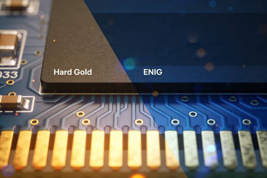
Because gold finger PCBs also require specific steps like nickel and hard‑gold electroplating, plating buses (tie‑bars), and precision beveling, we ensure that your panel layout is compatible with our plating lines and bevel equipment. For example, we verify that there is enough straight edge for the connector side to be clamped and beveled cleanly, and that any plating bars used to feed current into the finger area can be routed off without leaving artifacts near the contacts.
If you are designing a new panel from scratch or converting a prototype into a production‑ready array, you can share your concept through our “Gold Finger PCB Fabrication & Manufacturing Service” page and request a panelization‑focused DFM review. Our engineers will help you choose between V‑scoring, tab‑routing, or hybrid approaches, decide where to place rails and tooling holes, and confirm that the final panel design supports both yield and connector reliability before you commit to larger builds.
Conclusion
Panelization and routing choices around gold fingers are just as important as the connector footprint or plating stack if you care about yield and long‑term reliability. By standardizing orientation, keeping tabs and V‑scores away from the connector edge, defining clear keep‑outs and routing bands, and treating high‑speed and power fingers as part of your controlled‑impedance path, you can prevent many of the problems that usually show up only after first articles are built.
The good news is that none of these improvements require exotic design tricks—only a deliberate checklist and alignment with how your PCB manufacturer actually builds gold finger panels. If you treat the connector edge as a critical feature in your DFM review rather than an afterthought, you will see fewer damaged bevels, cleaner contacts, and more usable boards per panel.
If you are working on a new gold finger PCB or want to turn a prototype into a production‑ready panel, you can send your files and basic requirements through our “Gold Finger PCB Fabrication & Manufacturing Service” page and request a panelization‑focused review. Share how the connector will be used and any constraints you have on size, cost, and lead time, and our engineering team will help you refine orientation, rails, tabs, and bevel details so your next build starts from a manufacturing‑friendly panel design.