
Semiconductor Package Substrates
IC Substrate Manufacturing
PCBELEC provides custom IC substrate manufacturing for BGA, CSP and flip-chip package requirements. Define the material system, interconnect structure and acceptance criteria with our team, from prototype builds to production orders.
Share your package requirements: sales@pcbelec.com
Package Substrate Projects
Match the Substrate to Your Package Requirements
PCBELEC supports custom bare IC substrate manufacturing for prototype and production projects. Start with the package drawing, connection requirements and material specification so the manufacturing scope can be defined.
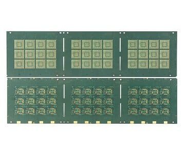
BGA Substrate Projects
Define the package-side connections, board-side ball map and substrate construction for your BGA package requirements.
Include: package outline, pad geometry, ball pitch, routing requirements and delivery format.
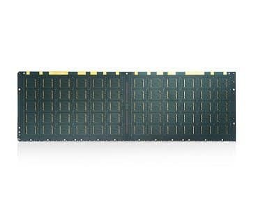
CSP Substrate Projects
Share the dimensional and interconnect requirements for your chip-scale package project, including the required substrate outline and finished thickness.
Include: die and package dimensions, connection layout, tolerances and handling requirements.
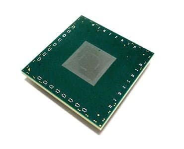
Flip-Chip Substrate Projects
Define the die-side pad arrangement, interconnect escape requirements and substrate stackup for the intended flip-chip package design.
Include: bump or pad map, surface finish requirements, build-up structure and coplanarity criteria.
Package format and interconnect method are separate decisions. BGA, CSP and flip-chip descriptions can overlap. Confirm the actual package construction rather than treating these labels as mutually exclusive manufacturing categories.
Discuss Your Package Requirements →Materials, Construction & Interconnects
Define the Manufacturing Specification
PCBELEC reviews material systems, layer construction and circuit requirements together. The applicable process, tolerances and verification scope are confirmed for the submitted package design.
Swipe horizontally if needed to view all specification details.
| Specification Area | Project Scope | Details to Confirm |
|---|---|---|
| Material System | BT resin-based laminates, ABF-based build-up structures, polyimide and specified high-performance laminates. | Material designation, grade, dielectric requirements, thermal properties and approved alternatives. |
| Ceramic Substrate Projects | Specified ceramic-based substrate requirements, reviewed as a distinct material and process route. | Ceramic composition, metallization, conductor definition, thickness, surface condition and acceptance criteria. |
| Layer Construction | Single-layer or multilayer circuit structures, including the specified core and build-up arrangement. | Stackup, layer sequence, dielectric thickness, copper requirements and finished substrate thickness. |
| Circuit & Pad Features | Fine-feature routing and connection patterns defined by the package design. | Line width and spacing, pad dimensions, pitch, copper thickness and dimensional tolerances. |
| Via Structure | Laser microvias, blind or buried vias and specified stacked or staggered interconnect arrangements. | Via map, diameter, depth, capture pads, filling requirements and the applicable structure for the material system. |
| Surface Finish & Openings | Specified finishes, including ENIG or ENEPIG where appropriate for the approved substrate construction. | Die-side and board-side finish requirements, plating thickness, mask or coverlay openings and downstream connection needs. |
| Geometry & Delivery Format | Individual substrates, strips or panels according to the agreed manufacturing and handling requirements. | Outline, datum references, alignment features, flatness or warpage limits, identification and packaging. |
| Verification & Records | Agreed dimensional inspection, circuit verification and project-specific checks. | Test method, measurement conditions, sampling requirements, acceptance limits and requested documentation. |
Requirements are reviewed as a complete structure. Listed materials and features are not interchangeable or automatically combinable. Final manufacturing limits, availability and lead time are confirmed against the design and accepted quotation.
Engineering Review Priorities
Resolve the Details That Define the Build
A package name alone does not define a manufacturable substrate. PCBELEC reviews the drawings, connection layouts and acceptance requirements together to identify details needing confirmation.
Start from a consistent design package. Identify the current revision and distinguish fixed requirements from preferences or preliminary information.
-
01
Die-Side & Board-Side Connections
Align the pad or bump map, connection geometry, routing requirements and reference orientation. Identify any differences between drawings and supplied circuit data.
Confirm: connection definitions and the files that govern each interface.
-
02
Materials, Stackup & Surface Requirements
Review the material grade, layer sequence, via arrangement, copper requirements and specified finishes as one construction, including conditions for any alternatives.
Confirm: the approved construction and any permitted substitutions.
-
03
Dimensions, Flatness & Handling
Define the outline, thickness, datum references and dimensional tolerances. Where flatness or warpage is specified, include the measurement conditions and acceptance limits.
Confirm: measurable limits and the required individual, strip or panel format.
-
04
Verification & Qualification Scope
Identify the required inspection, electrical checks, evaluation samples and documentation. Separate routine manufacturing checks from additional qualification work requested for the project.
Confirm: methods, sampling, acceptance criteria and the records included in the order.
Proposed design or process changes are submitted for confirmation before becoming part of the approved manufacturing specification.
Submit Your Project for Review →Manufacturing & Verification
Follow the Approved Manufacturing Route
The process route and verification plan follow the accepted material system, substrate construction and project requirements. Different structures do not automatically share the same manufacturing sequence.

-
01
Engineering & Release
Align the fabrication data, drawings, stackup and engineering answers. Establish the released revision and manufacturing specification.
-
02
Circuit & Interconnect Formation
Manufacture the circuit features, dielectric structure and interlayer connections using the process route confirmed for the material and design.
-
03
Finishing & Dimensional Control
Complete the specified surface treatment, protective openings and final format. Check the relevant geometry against the agreed limits and conditions.
-
04
Verification & Delivery Preparation
Complete the agreed inspection and electrical verification scope, then prepare the required identification, records and protective packaging.
Additional qualification, reliability evaluation or customer-specific testing should be identified before quotation and included in the accepted scope where required.
Explore Testing & Inspection →Prepare Your Substrate Project
Share a Clear Manufacturing Package
Send the available design data with the package requirements and project stage. Identify what is fixed, what is preliminary and where you need engineering input.
Design Data & Revision
Fabrication data, drawings, connection maps, orientation references and the current revision. List the files that govern the design.
Materials & Construction
Material grades, stackup, finished thickness, conductor and via requirements, surface finishes and permitted alternatives.
Acceptance & Documentation
Dimensional limits, flatness or warpage criteria, verification methods, qualification requirements and requested records.
Quantity & Delivery
Prototype or production quantity, individual or panel format, packaging, destination and target ship or arrival date.
Preliminary inquiries are welcome. A firm quotation and manufacturing release may require additional information. Review the manufacturing file guide for general preparation, and include any package-specific data requirements separately.
IC Substrate FAQ
Clarify Your Project Before Release
Practical answers about project scope, materials, manufacturing requirements and quotation preparation.
Which IC substrate projects can I discuss with PCBELEC?
Submit your BGA, CSP or flip-chip substrate requirements, including the intended construction, material system and project stage. PCBELEC supports prototype and production inquiries for custom bare package substrates.
The applicable manufacturing route and acceptance scope are confirmed against the design rather than the package label alone.
Can I specify BT, ABF, polyimide or ceramic materials?
Yes. Include the required material grade, construction and performance criteria, together with any approved alternatives.
These material systems are reviewed within their respective process routes. They should not be treated as direct substitutes without confirming the design and manufacturing implications.
What line width, spacing and via limits apply?
Provide the required dimensions and tolerances with the material system, copper specification, stackup and via arrangement. The applicable limits need confirmation for that complete structure.
Do not assume that a minimum value quoted for one construction also applies to every material, layer arrangement or feature combination.
Can I request a preliminary review before all files are final?
Yes. Send the available drawings, connection maps, material preferences and target quantity. Mark preliminary items and identify where engineering input is needed.
A firm quotation or manufacturing release may require additional data and an approved final revision.
How are prototype quantity and lead time confirmed?
State the required sample or production quantity, delivery format and target date. Quantity conditions and timing are confirmed in the project quotation.
Identify whether the deadline is a ship date or an arrival date. Materials, engineering approvals and additional verification requirements are considered when agreeing the schedule.
Can customer-specific tests and records be included?
Identify the required test methods, measurement conditions, sampling, acceptance limits and documentation before quotation.
Additional qualification or reliability work requires an agreed scope. It should not be assumed to be included in routine manufacturing verification.
How should I submit confidential design information?
Contact sales@pcbelec.com before sending restricted files if your project requires an NDA or a specified transfer arrangement.
Confirm the required arrangements before disclosure. General personal-data information is provided in the Privacy Policy .