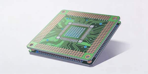
Multilayer PCB Manufacturing Services in China
High‑reliability multilayer PCB manufacturing from a trusted China‑based supplier – supporting 4–30 layers, rigid, flex and rigid‑flex boards for demanding industrial, telecom, medical, and aerospace applications.
- 4–30 Layer Capability – Custom multilayer stack‑ups for complex designs and high‑density routing.
- Rigid, Flex & Rigid‑Flex Options – One supplier for your multilayer rigid, flexible, and rigid‑flex PCB needs.
- Engineering & DFM Support – Gerber review, stack‑up suggestions, and manufacturability checks before production.
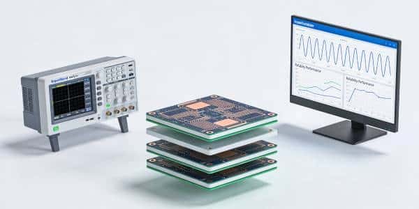
- Stable Quality & Testing – Impedance control, flying‑probe and AOI testing ensure reliable performance.
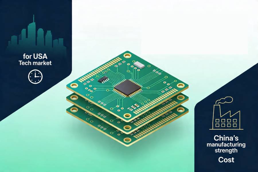
- Competitive China Manufacturing – Cost‑effective multilayer PCB fabrication without compromising quality.
Typical lead times available for low‑volume and production orders. Engineering files are kept strictly confidential.
Why Choose JHYPCB for Multilayer PCB Manufacturing
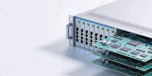
JHYPCB provides custom multilayer PCB manufacturing services for customers who need stable quality, engineering support, and dependable production capability. As a China-based PCB manufacturer, we support a wide range of multilayer rigid, flex, and rigid-flex PCB requirements for industrial, telecom, medical, automotive, and other demanding applications.
01
15+ Years of Manufacturing Experience
Extensive experience in multilayer PCB fabrication for complex and reliability-critical applications.
02
Engineering Review & DFM Support
Gerber review and manufacturability checks help reduce errors before production starts.
03
Rigid, Flex & Rigid-Flex Capability
One supplier for a wide range of multilayer PCB structures and application needs.
04
Stable Quality Control
AOI, electrical testing, and process control support consistent multilayer PCB quality.
05
Custom Stack-Up Support
Support for different materials, layer counts, and technical requirements based on project needs.
06
Competitive China Manufacturing
Cost-effective production backed by experienced manufacturing and supply chain advantages.
Multilayer PCB Manufacturing Capabilities at JHYPCB
JHYPCB supports a wide range of multilayer PCB manufacturing requirements, from standard industrial products to more demanding applications that need higher layer counts, controlled impedance, or special materials. The overview below summarizes our main multilayer PCB fabrication capabilities.
| Feature | Specifications |
|---|---|
| Layer Count | Rigid multilayer PCBs: up to 32 layers Flexible multilayer PCBs: up to 10 layers Rigid-flex multilayer PCBs: up to 8 layers |
| Board Types | Rigid multilayer PCB, multilayer flex PCB, and rigid-flex multilayer PCB |
| Base Materials | Rigid: FR4, high-Tg FR4, and selected high-frequency materials Flexible / Rigid-flex: polyimide-based constructions |
| Finished Board Thickness | Rigid: 0.4–6.0 mm Flexible: 0.1–0.8 mm Rigid-flex: 0.25–2.0 mm |
| Copper Weight | Multiple copper thickness options are available for inner and outer layers based on current-carrying, thermal, and design requirements |
| Solder Mask Options | Standard colors such as green, white, black, blue, and other options on request |
| Surface Finishes | Lead-free HASL, ENIG (immersion gold), immersion silver, immersion tin, hard gold, and other finishes on request |
| Testing & Inspection | Electrical testing, flying-probe testing, AOI, and additional checks such as solderability testing, thermal shock, and impedance verification when required |
If your project requires a specific stack‑up, material combination, or additional technical details beyond the capabilities listed here, our engineering team can review your design files and confirm the most suitable multilayer PCB manufacturing approach.
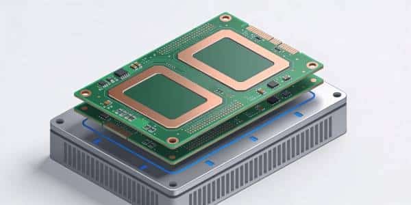
Types of Multilayer PCB We Can Manufacture
JHYPCB can manufacture different types of multilayer PCBs to match the mechanical, electrical, and assembly requirements of your project. From standard rigid multilayer boards to flexible and rigid-flex constructions, our team can help you select the most suitable multilayer PCB structure for your application.
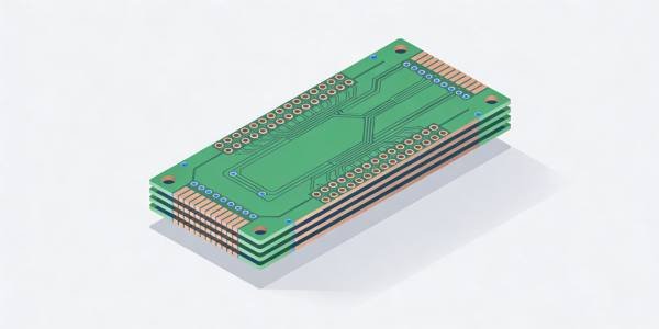
Rigid multilayer PCBs are the most widely used option for products that require stable structure, reliable interconnection, and consistent electrical performance. JHYPCB manufactures rigid multilayer PCBs with different layer counts, materials, and stack-up options for industrial, telecom, computing, and other demanding applications.
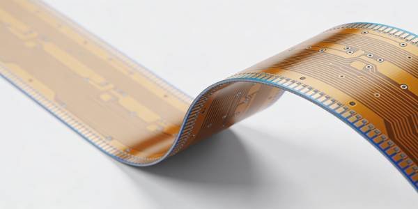
Flexible multilayer PCBs are designed for applications that require bending, folding, or installation in limited spaces. We manufacture multilayer flex PCBs using polyimide-based constructions to support compact designs, reduce wiring complexity, and improve assembly flexibility.
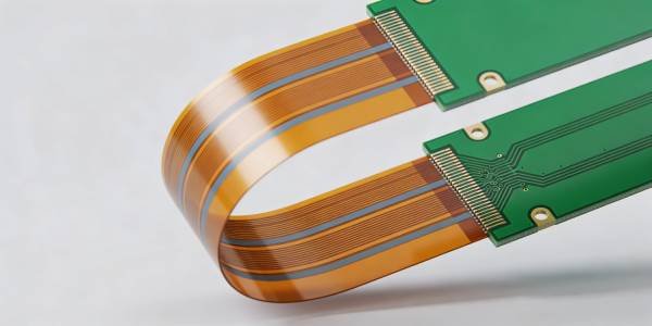
Rigid-flex multilayer PCBs combine rigid sections for component mounting with flexible sections for interconnection in a single board structure. JHYPCB provides rigid-flex multilayer PCB manufacturing for applications that need space savings, improved reliability, and better resistance to vibration and mechanical stress.
HDI multilayer PCBs are built for high-density designs that require finer lines, smaller vias, and more complex routing in limited board space. We support HDI multilayer PCB manufacturing for projects that need compact layouts, higher I/O density, and improved signal performance.
Metal-based multilayer PCBs are suitable for applications that require improved heat dissipation and stable thermal performance. JHYPCB can manufacture metal-based multilayer PCB solutions for power electronics, LED systems, and other products with higher thermal management requirements.
High-frequency and high-speed multilayer PCBs are used in designs where signal integrity, impedance control, and material performance are critical. We support the manufacturing of high-frequency and high-speed multilayer PCBs for RF, microwave, telecom, and fast digital applications with more demanding electrical requirements.
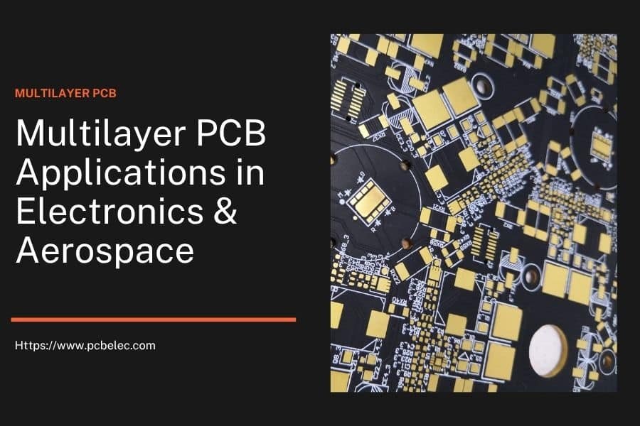
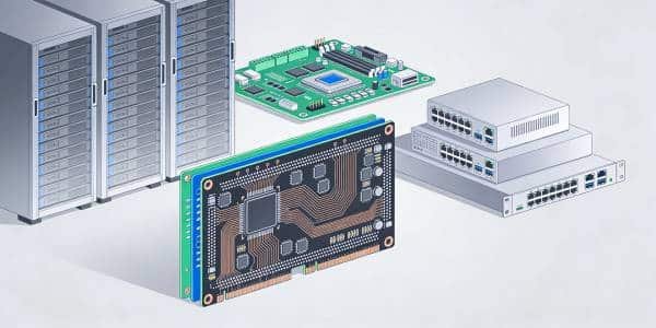
Industries We Serve with Multilayer PCB Manufacturing
JHYPCB manufactures multilayer PCBs for a wide range of industries that require higher circuit density, reliable electrical performance, and stable manufacturing quality. Our multilayer PCB solutions are used in products where compact design, signal integrity, durability, and long-term consistency are critical.
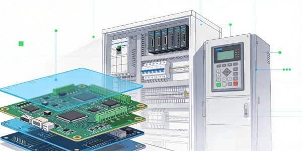
Industrial Control
Multilayer PCBs for industrial control equipment need stable performance, durable construction, and long-term reliability in demanding operating environments. JHYPCB supports multilayer PCB manufacturing for industrial electronics that require dependable interconnection and consistent production quality.
Telecommunication
Telecommunication equipment often requires multilayer PCB designs with higher routing density, better signal integrity, and reliable electrical performance. We manufacture multilayer PCBs for telecom and networking applications where stable transmission and controlled board quality are important.
Medical Devices
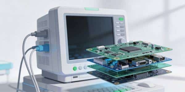
Medical electronics require multilayer PCBs with high reliability, precise manufacturing control, and consistent quality from batch to batch. JHYPCB supports multilayer PCB production for medical applications that demand compact design, stable signals, and dependable performance.
Aerospace & Defense
Aerospace and defense applications often involve complex multilayer PCB structures, limited installation space, and strict reliability expectations. We provide multilayer PCB manufacturing for high-performance electronic systems that require robust construction and dependable layer-to-layer connectivity.
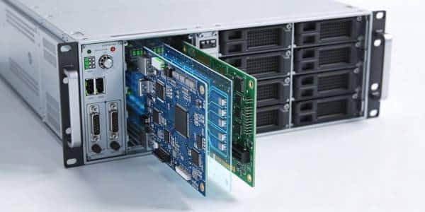
Computing & Data Systems
Computing products and embedded data systems use multilayer PCBs to support more complex circuits, higher component density, and efficient signal routing in compact board layouts. JHYPCB manufactures multilayer PCBs for computing applications that require stable structure and reliable electrical connection.

Wearable & Compact Electronics
Wearable and compact electronic products rely on multilayer PCBs to integrate more functionality into smaller spaces. Our multilayer PCB manufacturing supports compact designs where board size, weight, and routing efficiency all need to be carefully balanced.
If your industry has specific electrical, mechanical, or reliability requirements, our engineering team can review your project and recommend a suitable multilayer PCB structure, material system, and manufacturing approach.
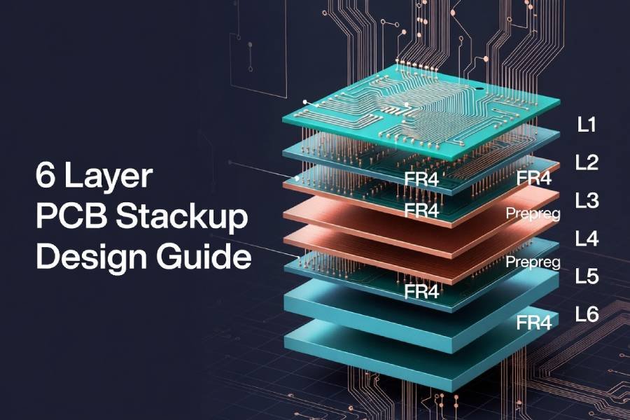
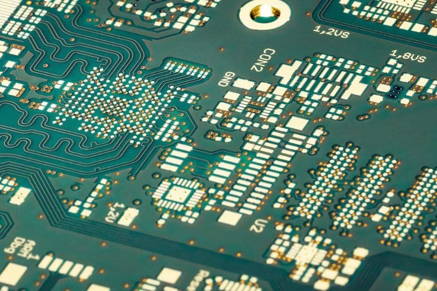
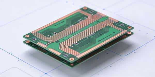
What Is a Multilayer PCB?
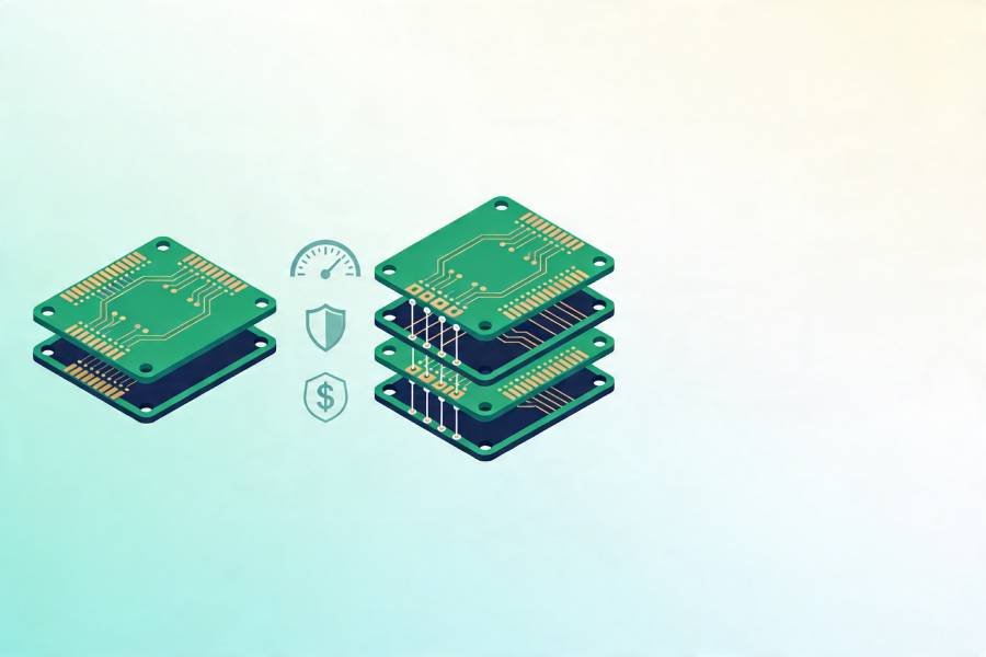
A multilayer PCB is a printed circuit board built with three or more conductive copper layers separated by insulating material and laminated into a single structure. Compared with single-sided or double-sided boards, multilayer PCBs provide more routing space, higher circuit density, and better support for complex electronic designs.
In a typical multilayer PCB, components are mounted on the outer layers, while the inner layers are used for signal routing, power distribution, and ground planes. This structure helps improve layout efficiency, reduce board size, and support better electrical performance in products with more demanding circuit requirements.
Multilayer PCBs are widely used in applications where compact size, signal integrity, and functional integration are important, including industrial equipment, medical devices, telecom systems, aerospace electronics, and other advanced products. JHYPCB provides custom multilayer PCB manufacturing for customers who need reliable fabrication support for these more complex board designs.
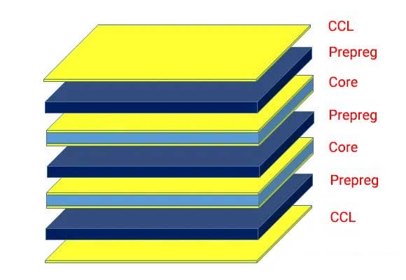
Typical multilayer PCB structure with outer layers for component mounting and inner layers for routing and electrical connectivity.
Why Use Multilayer PCBs?
Multilayer PCBs are used when a design requires more routing space, higher circuit density, and better electrical organization than single-sided or double-sided boards can provide. As electronic products become smaller and more functionally complex, multilayer PCB structures help engineers integrate more circuitry into a compact and reliable board design.
Higher Circuit Density
Multilayer PCBs allow more circuits to be routed within a limited board area by using multiple conductive layers inside a single structure. This makes them suitable for products that need more functions, more components, and more complex interconnections without increasing overall board size.
More Compact Product Design
Compared with single-sided or double-sided boards, multilayer PCBs help reduce the footprint of the final assembly. By using inner layers for routing, power, and ground, designers can build more compact products while keeping the layout more organized and efficient.
Better Electrical Performance
A multilayer board structure can support improved signal routing, better grounding, and more effective power distribution. In many applications, this helps improve signal integrity, reduce interference, and support more stable electrical performance in complex circuits.
Greater Design Flexibility
Multilayer PCBs give engineers more freedom when working with dense layouts, high pin-count components, and performance-driven designs. This added routing flexibility is especially important in products where board space is limited but electrical requirements are more demanding.
Improved Reliability for Complex Electronics
Because multilayer PCBs are designed as a single laminated structure, they can provide reliable interconnection across more advanced circuit designs. For many industrial, medical, telecom, and aerospace applications, this makes multilayer PCB technology a practical solution for more demanding products.
Single-sided and double-sided PCBs remain useful for simpler electronics, but they become less efficient when the design requires higher component density, more routing channels, or more advanced electrical performance. In these cases, multilayer PCBs provide a more practical and scalable solution.
| Aspect | Single-/Double-Sided PCB | Multilayer PCB |
|---|---|---|
| Circuit Complexity | Better suited to simple or less dense circuits | Better suited to complex and high-density circuit designs |
| Space Efficiency | Requires more board area as routing demand increases | Uses inner layers to achieve more compact layouts |
| Routing Flexibility | Limited routing space and fewer interconnection options | Greater routing freedom across multiple internal layers |
| Electrical Performance | More limited control of grounding, power distribution, and signal routing | Better support for signal integrity, grounding, and power organization |
| Typical Applications | Basic consumer, simple control, and lower-complexity products | Advanced industrial, medical, telecom, aerospace, and embedded systems |
If your product requires a compact layout, more complex routing, or more stable electrical performance, multilayer PCB fabrication is often the more effective choice than a simpler board structure. JHYPCB supports custom multilayer PCB manufacturing for projects that need reliable production and engineering support.
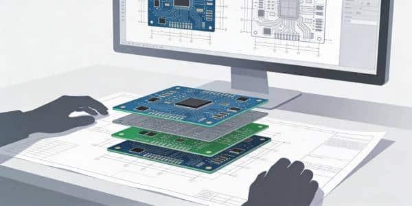
Multilayer PCB Manufacturing Process
Multilayer PCB manufacturing requires precise control at every stage, from engineering review and inner-layer processing to lamination, drilling, plating, and final inspection. At JHYPCB, each step is managed to support stable layer alignment, reliable interconnection, and consistent board quality for demanding multilayer PCB applications.
1.
Engineering Review
The process starts with engineering review of the design data, stack-up requirements, and manufacturing details before production begins. This step helps confirm manufacturability, reduce avoidable risks, and prepare the board for stable multilayer PCB fabrication.
2.
Material Preparation
Suitable base materials are selected according to the board structure and project requirements, such as FR4, high-Tg materials, polyimide, or other specified laminates. Material preparation is an important part of ensuring the board meets mechanical, electrical, and thermal expectations.
3.
Inner Layer Fabrication
Inner layers are imaged and etched to form the required circuit patterns before lamination. Accuracy at this stage is essential because the inner layers define much of the routing, power distribution, and grounding structure of the final multilayer PCB.
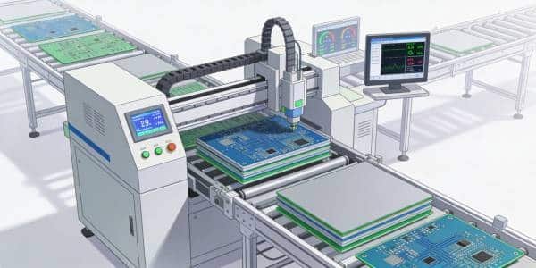
4.
Lamination and Drilling
The processed copper layers and prepreg materials are laminated under controlled heat and pressure to form a single multilayer structure. After lamination, drilling is performed to create vias and holes that will enable electrical interconnection between layers.
5.
Plating and Outer Layer Processing
Plating is used to build conductive connections through vias, while the outer layers are processed to form the final circuit pattern. This stage directly affects layer-to-layer connectivity, routing accuracy, and the overall electrical performance of the board.
6.
Solder Mask and Surface Finish
A solder mask is applied to protect the circuitry and reduce the risk of shorts or contamination during assembly and use. Surface finishes such as lead-free HASL, ENIG, immersion silver, immersion tin, or hard gold are then applied according to product and assembly requirements.
7.
Electrical Testing and Final Inspection
Before shipment, multilayer PCBs go through electrical testing and final inspection to verify connectivity, detect faults, and confirm overall manufacturing quality. Depending on the project, inspections may include AOI, flying-probe testing, impedance checks, and other verification steps.
This controlled manufacturing process helps ensure that each multilayer PCB is built to meet the structural, electrical, and reliability requirements of the intended application. For projects with more specific technical demands, JHYPCB can further review stack-up, material, and testing requirements based on your design files.
Quality Control for Multilayer PCB Manufacturing
Multilayer PCB manufacturing requires more than standard fabrication control, because layer alignment, via reliability, material consistency, and electrical performance all have a direct impact on the finished board. At JHYPCB, quality control is applied throughout the manufacturing process to help ensure each multilayer PCB meets the required structural and electrical standards.
Engineering Review Before Production
Quality control begins before fabrication starts. Our engineering team reviews design files, stack-up requirements, and manufacturing details in advance to identify potential issues that could affect manufacturability, reliability, or production yield.
Process Control During Manufacturing
Each major manufacturing stage, including inner-layer processing, lamination, drilling, plating, and outer-layer formation, is managed under controlled production conditions. This helps maintain layer-to-layer accuracy, stable interconnection quality, and consistent board construction.
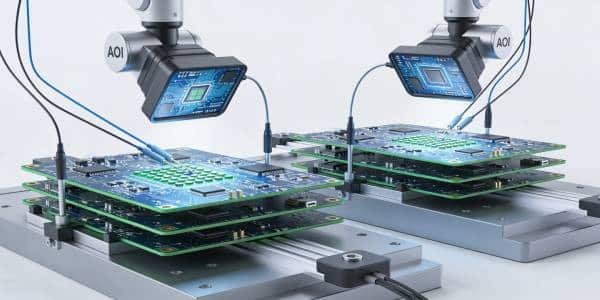
Optical and Electrical Inspection
To verify circuit accuracy and finished board performance, multilayer PCBs go through inspection and testing procedures such as automated optical inspection (AOI) and electrical testing, including flying-probe testing when required. These checks help detect opens, shorts, and other manufacturing defects before shipment.
Verification for Technical Requirements
For projects with more demanding electrical or reliability requirements, additional verification can be applied according to product needs. Depending on the design, this may include impedance control, solderability checks, thermal shock testing, or other reliability-focused inspections.
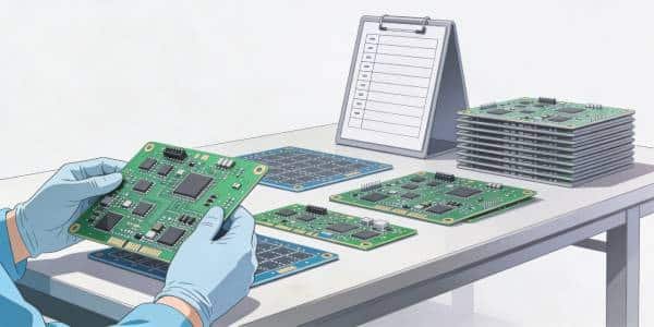
Final Inspection Before Delivery
Before delivery, finished multilayer PCBs go through final inspection to confirm that the boards meet manufacturing and quality requirements. This final step helps ensure the product is ready for assembly and end-use application.
By combining engineering review, in-process control, testing, and final inspection, JHYPCB works to provide multilayer PCB manufacturing with stable quality and dependable performance. If your project includes special quality, testing, or reliability requirements, our team can review them together with your design files before production.
Multilayer PCB FAQs
Find answers to common questions about multilayer PCB manufacturing, materials, technical options, and quotation requirements. If you need additional support, our team can review your project requirements and provide a suitable manufacturing recommendation.
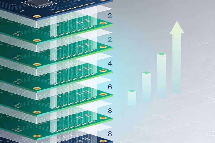
JHYPCB supports rigid multilayer PCBs up to 30 layers, flexible multilayer PCBs up to 10 layers, and rigid-flex multilayer PCBs up to 8 layers. The suitable layer count depends on your design complexity, electrical requirements, and board structure.
Available material options include standard FR4, high-Tg FR4, selected high-frequency materials, and polyimide-based constructions for flex and rigid-flex multilayer PCBs. Material selection depends on the thermal, mechanical, and electrical requirements of the project.
Yes. JHYPCB manufactures rigid multilayer PCBs, multilayer flex PCBs, and rigid-flex multilayer PCBs for different application needs. This allows customers to choose the most suitable structure based on space, flexibility, and performance requirements.
JHYPCB supports a range of surface finishes, including lead-free HASL, ENIG, immersion silver, immersion tin, and hard gold. The most suitable finish depends on assembly method, performance requirements, and product application.
Yes. Impedance control can be supported for multilayer PCB projects that require more demanding signal performance. If impedance is required, it should be clearly specified in the design files or project documentation before production.
In most cases, Gerber files and basic manufacturing requirements are needed to prepare an accurate quotation. If the project includes special stack-up, material, impedance, or testing requirements, these details should also be provided for engineering review.
Quality control is applied throughout the manufacturing process through engineering review, process control, AOI, electrical testing, and final inspection. Depending on the project, additional verification such as flying-probe testing, solderability checks, thermal shock testing, or impedance verification may also be used.
Yes. In addition to multilayer PCB fabrication, JHYPCB also provides PCB assembly services for customers who need a more complete manufacturing solution. If assembly is required, please share your project details together with the PCB design files so our team can review the manufacturing and assembly requirements.
If you have additional questions about multilayer PCB manufacturing, materials, stack-up options, or testing requirements, please contact our team for project-based support. You can also send your Gerber files for quotation and engineering review.

Get a Quote for Your
Multilayer PCB Project
JHYPCB provides custom multilayer PCB manufacturing for customers who need reliable quality, engineering support, and stable production capability. Send your Gerber files and project requirements to receive a quotation and manufacturing review.