


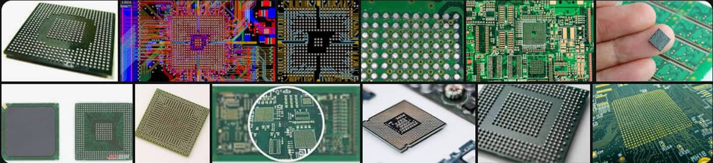
Ball Grid Array (BGA) PCB Manufacturing & Assembly Services
High-reliability BGA PCB manufacturing and assembly with fine-pitch capability, 100% X-ray inspection, and rapid turnaround from prototypes to volume production.
- Fine-pitch BGA and µBGA assembly for high-density designs.
- 100% X-ray inspection of all BGA solder joints.
- DFM support for BGA PCB layout, fan-out, and via-in-pad design.
- Prototype, small-batch, and volume BGA PCB manufacturing and assembly services.
- BGA rework and reballing services for complex boards.

What Is BGA (Ball Grid Array) and Why It Matters for Your PCB?
A ball grid array (BGA) is a high-density surface-mount package that uses an array of solder balls on the underside of the component instead of traditional leads. It is widely used in advanced electronics such as processors, FPGAs, ASICs, memory, and high-speed communication devices where compact size and high I/O counts are required.
- Higher I/O density in a smaller footprint compared to QFP and other leaded packages.
- Improved electrical performance and signal integrity for high-speed, high-frequency designs.
- Better thermal performance and heat dissipation through the solder ball array and internal structure.
- Increased mechanical reliability when assembled with a controlled reflow process and proper PCB design.
Today, BGA packages are standard in smartphones, networking equipment, automotive control units, industrial automation systems, and many other compact, high-performance electronic products. Choosing the right BGA PCB manufacturing and assembly partner is critical to ensure long-term reliability and consistent yield.
BGA PCB Manufacturing & Assembly Capabilities
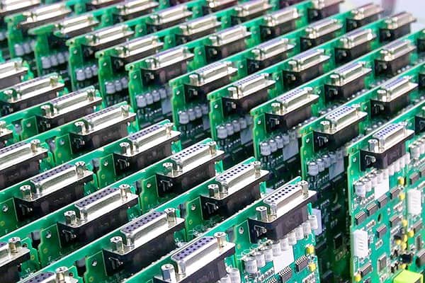
JHYPCB provides comprehensive BGA PCB manufacturing and assembly services for fine-pitch, high-density designs. Our capabilities cover standard BGA, micro BGA, and complex multi-BGA boards, backed by controlled PCB fabrication, advanced SMT lines, and 100% X-ray inspection of all BGA solder joints.
| Item | Capability (Typical Values / Range) |
|---|---|
| BGA package types | PBGA, CBGA, FBGA, micro BGA, stacked BGA, PoP (package-on-package) |
| Minimum BGA pitch | Down to 0.25 mm (fine-pitch BGA and µBGA) |
| Supported PCB layers | Up to 40 layers for BGA-based high-density multilayer PCBs |
| Board thickness range | Typically 0.4 mm – 3.2 mm (custom thickness on request) |
| Min trace/space for BGA breakout | Down to 2.5/2.5 mil (0.063/0.063 mm) with HDI stack-ups |
| Via technology | Through-hole, laser-drilled microvias, stacked and staggered microvias, via-in-pad (filled and capped) for fine-pitch BGAs |
| Surface finishes | ENIG, ENEPIG, immersion tin, immersion silver, lead-free HASL, hard gold / soft gold for edge connectors and special applications |
| BGA assembly volume | Prototypes (1–50 pcs), small to medium batches, and mass production |
| Placement accuracy | High-speed SMT placement with ±25 µm accuracy (3σ) for fine-pitch BGAs |
| Inspection & testing | 100% X-ray inspection for all BGAs, 3D AOI, ICT and functional testing available according to customer requirements |
| Rework & reballing | Precision BGA rework, replacement, and reballing services with dedicated BGA rework stations and X-ray verification |
With these capabilities, JHYPCB can reliably handle complex BGA-based PCBs from early prototypes to stable volume production, while our engineering team supports you with DFM reviews and optimized processes for consistent quality and yield.
BGA PCB Manufacturing & Assembly Process
To ensure reliable BGA solder joints and consistent yield, JHYPCB follows a tightly controlled end-to-end process for BGA PCB manufacturing and assembly. From DFM review and HDI fabrication to optimized reflow profiles and 100% X-ray inspection, every step is engineered for quality.
By combining rigorous process control with advanced equipment, JHYPCB helps you reduce BGA-related field failures and accelerate time-to-market for your high-performance electronic products.
BGA PCB Design & DFM Guidelines
Reliable BGA PCB assembly starts with a manufacturable PCB design. To help you avoid costly respins and BGA solder issues, JHYPCB’s engineering team provides DFM support and practical design guidelines for BGA pad geometry, fan-out, via structures, and solder mask design.
1. BGA Pad Design & Land Pattern
- Follow the component manufacturer’s recommended land pattern for each specific BGA package.
- Use non-solder mask defined (NSMD) pads for most BGAs to achieve better solder joint reliability and more consistent pad dimensions.
- Ensure adequate pad-to-pad spacing to accommodate solder mask and prevent bridging between neighboring balls.
2. Fan-Out Strategy & Escape Routing
- For BGA pitches ≥ 0.65 mm, traditional dog-bone fan-out with vias placed just outside the pad ring is typically sufficient.
- For 0.4–0.5 mm pitch BGAs, consider using microvias in the “dog-bone” or between pads, combined with HDI stack-ups to escape inner rows.
- For ultra-fine pitch (≈0.3–0.25 mm), via-in-pad with filled and capped vias is often required to route signals while maintaining controlled impedance and manufacturability.
3. Via-in-Pad & Solder Mask Considerations
- When using via-in-pad for BGAs, ensure vias are properly filled and capped to prevent solder wicking and voids under the balls.
- Avoid open through-holes on BGA pads; instead, use tented or covered vias away from pads if via-in-pad is not required.
- Carefully define solder mask openings to balance solder spread, avoid mask slivers, and maintain sufficient dam between adjacent pads.
4. Stack-Up, Power Integrity & Thermal Management
- Use solid reference planes under BGA areas to control impedance and reduce noise for high-speed signals.
- Place decoupling capacitors as close as possible to BGA power/ground balls, typically on the back side directly under the BGA with short via connections.
- Add thermal vias under hot BGAs to spread heat into internal copper planes and improve overall thermal performance.
5. Design for Inspection & Rework
- Maintain sufficient clearance around BGAs to allow effective X-ray inspection and potential rework operations.
- Avoid placing tall components too close to BGA edges, which can shadow X-ray images or interfere with hot-gas nozzles on rework equipment.
- Clearly mark BGA pin 1 and orientation on the silkscreen to reduce assembly and debugging errors.
If you share your BGA PCB design files early, JHYPCB can review your layout and provide tailored DFM recommendations to improve manufacturability, yield, and long-term reliability before you commit to volume production.
BGA Quality Control & Inspection
Because BGA solder joints are hidden under the package body, robust inspection and process control are essential to avoid latent defects. JHYPCB combines optimized reflow profiles, 100% X-ray inspection, 3D AOI, and optional electrical testing to ensure that every BGA PCB assembly meets your reliability requirements.
By combining advanced inspection technologies with disciplined process control, JHYPCB helps you minimize BGA-related field failures and build confidence in every production run.
Industries & Applications for BGA PCB Assemblies
BGA packages are used across many high-performance electronic products that demand compact size, high I/O density, and reliable high-speed interconnects. JHYPCB supports BGA PCB manufacturing and assembly for a wide range of industries and end applications.
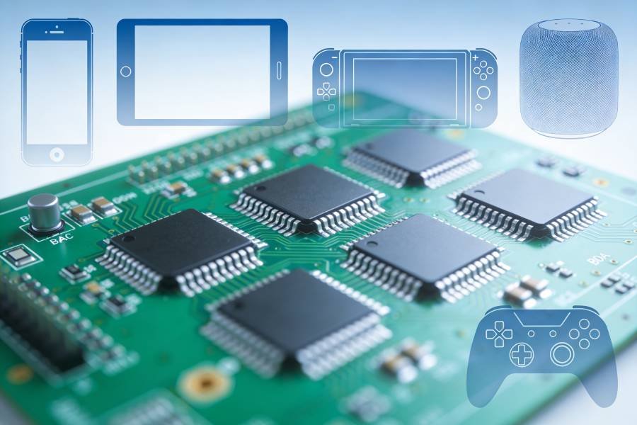
Consumer Electronics
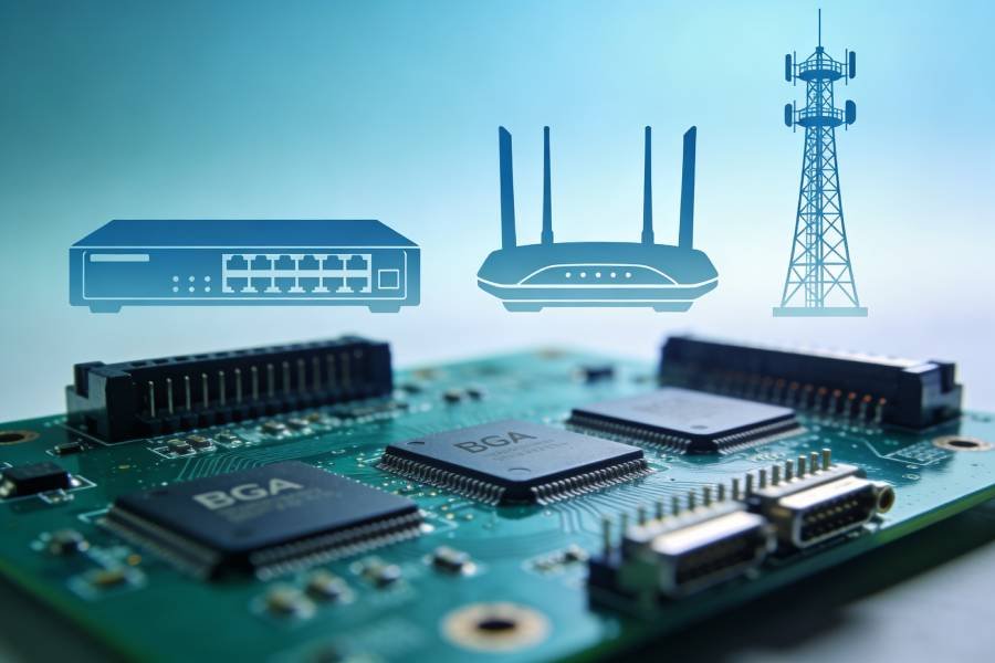
Networking & Telecom
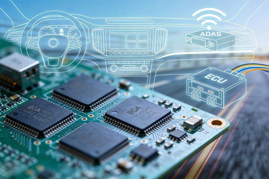
Automotive & Transportation

Industrial Control & Automation
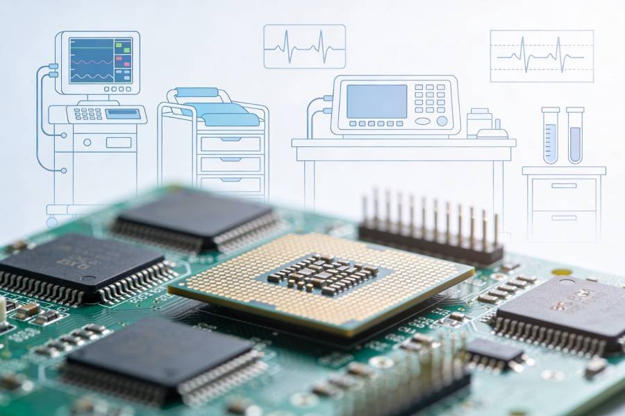
Medical & Instrumentation
Whether you are developing consumer devices, communication systems, automotive electronics, or specialized industrial and medical equipment, JHYPCB can tailor BGA PCB manufacturing and assembly solutions to meet your performance, reliability, and cost targets.
BGA PCB Pricing, Lead Time & Quote Requirements
BGA PCB manufacturing and assembly costs depend on board complexity, BGA pitch and count, HDI structures, component mix, testing requirements, and requested lead time. JHYPCB offers competitive pricing for both rapid prototypes and volume BGA production, with flexible options to match your schedule and budget.
Typical Lead Time for BGA PCB Assembly
- Prototypes and small runs: Typically 7–10 working days after all materials and data are confirmed.
- Complex HDI BGA boards (e.g. ≥ 10 layers, fine-pitch via-in-pad): Typically 10–15 working days depending on stack-up and testing requirements.
- Volume production: Standard lead times are usually agreed case-by-case based on order quantity and supply chain conditions.
Key Cost Drivers for BGA PCB Manufacturing & Assembly
- PCB complexity: layer count, HDI structure, microvias, via-in-pad, controlled impedance stack-up.
- BGA details: number of BGA components per board, ball count, minimum pitch, and required X-ray inspection level.
- Components & sourcing: BOM mix (standard vs. special parts), supply chain availability, and whether you provide any consigned parts.
- Testing & quality requirements: ICT, functional testing, burn-in or higher IPC class standards.
- Lead time: expedited or quick-turn services will typically carry a premium compared to standard schedules.
Request a Quote – Required Files & Information
To prepare an accurate BGA PCB manufacturing and assembly quote, please provide:
- Gerber or PCB design files (including drill files and stack-up information, if available).
- Bill of materials (BOM) with manufacturer part numbers, designators, quantities, and any approved alternates.
- Pick-and-place / XY data (or CAD data) for SMT programming and accurate BGA placement.
- Assembly drawings or PDF documentation highlighting critical components, special instructions, and testing requirements.
- Target quantity (prototype, pilot run, or volume) and desired lead time or delivery date.
Share your project files via our online quote form, and JHYPCB’s engineering and sales team will review your BGA PCB requirements and provide a detailed quotation and schedule proposal as quickly as possible.
FAQ about BGA PCB Manufacturing & Assembly
BGA packages are ideal when you need high I/O counts, compact board area, better electrical performance, and improved thermal characteristics. They are commonly used for processors, FPGAs, ASICs, and high-speed communication devices where traditional leaded packages cannot provide sufficient pin density or signal integrity.
For an accurate quote, we typically need your Gerber or PCB design files, BOM with manufacturer part numbers, pick-and-place/XY data, assembly drawings or special instructions, target quantities, and desired lead time. If you have specific testing or reliability requirements, please include those details as well.
We combine optimized reflow profiles with 100% X-ray inspection of all BGA components, supported by 3D AOI and optional electrical testing. X-ray allows us to detect voids, opens, shorts, head-in-pillow defects, and misalignment that cannot be seen optically, significantly improving reliability.
Yes, we support fine-pitch BGAs down to approximately 0.25 mm pitch using HDI stack-ups, microvias, and via-in-pad technology where required. Our high-precision SMT equipment and process controls are designed to handle micro BGA and high-density BGA layouts reliably.
We recommend using NSMD pads for most BGAs, appropriate fan-out strategies based on pitch (dog-bone for ≥0.65 mm, microvias/via-in-pad for finer pitches), properly filled and capped via-in-pad structures, solid reference planes, and careful solder mask definition. Our engineers can review your layout and provide DFM feedback before fabrication.
JHYPCB can provide BGA rework, replacement, and reballing using dedicated rework stations and X-ray verification. For high-reliability products, we follow industry best practices and limit the number of rework cycles per device location to protect pad integrity and long-term reliability.
Common BGA issues include solder voids, head-in-pillow, opens, shorts, and warpage-related misalignment. We mitigate these risks through proper stencil design, solder paste selection, controlled reflow profiles, accurate placement, and comprehensive X-ray inspection to catch and correct problems quickly.
Yes, we support the full lifecycle from early prototypes and engineering validation builds through pilot runs and mass production. Using the same BGA-capable processes and inspection standards across all volumes helps you de-risk scale-up and maintain consistent quality.

Request a Quote
Ready to Start Your BGA PCB Project?
Whether you are developing a new high-density prototype or scaling an existing design to volume production, JHYPCB is ready to support your BGA PCB manufacturing and assembly needs. Our engineers can review your design, optimize for manufacturability, and help you bring reliable BGA-based products to market faster.
- Advanced HDI PCB fabrication and fine-pitch BGA assembly.
- 100% X-ray inspection and robust process control for every BGA.
- Support from early prototypes to mass production.
Upload your Gerber, BOM, and pick-and-place files, and our team will respond with a detailed quotation and lead time estimate as soon as possible.
BGA PCB Design Guide, Assembly and Soldering Videos
How to fanout a BGA – Altium Designer 16.1
BGA Soldering
Ball Grid Array Rework: Package on Package Devices
How to inspect BGA Soldering performance on PCB
Recommended PCB Manufacturing Services


Related PCB Assembly Services


Helpful Resources
- JHYPCB Manufacturing Capabilities Introduction
- JHYPCB Factory Introduction
- How to Choose the Right PCB Manufacturer and Supplier
- PCB and PCBA Manufacturing Files
- The most comprehensive Introduction of Solder Resist for PCB
- What is the difference between SMT and SMD?
- What is the difference between wave soldering and reflow soldering?