
Color, Coverage & Precision for Custom PCB Fabrication
PCB Solder
Mask Options
Give your next board the appearance and solder mask construction it needs. PCBELEC brings color, material and pad-opening requirements into custom bare PCB manufacturing , with practical engineering support from prototype to production.
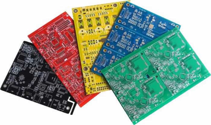
- Green, red, blue, yellow, white and black solder mask options for your board appearance.
- Engineering support for openings, mask dams, registration and via-protection requirements.
- Material and inspection requirements coordinated with the complete PCB construction.
Send your board files to sales@pcbelec.com
- Board Appearance Colors & Markings
- Engineering Details Openings & Registration
- Manufacturing Support Prototypes to Production
Real Board Examples, Clear Color Choices
What Color of Solder Mask Is Used on the PCB?
Green is a familiar choice, but it is not the only option. PCBELEC offers multiple solder mask colors so the board's appearance, markings and manufacturing requirements can work together.
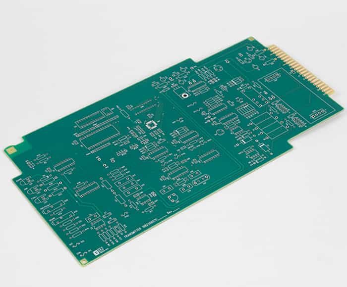
Green Solder Mask
A familiar board appearance for prototypes and production. Pair the mask with clear legend, identification and pad openings for the complete manufacturing build.
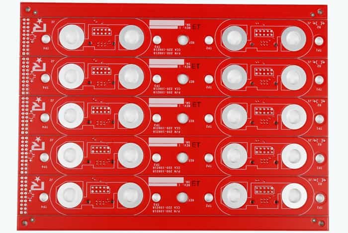
Red Solder Mask
Give the board a distinctive visual identity. Red can support product styling or board-variant identification, with markings and exposed features defined in the artwork.
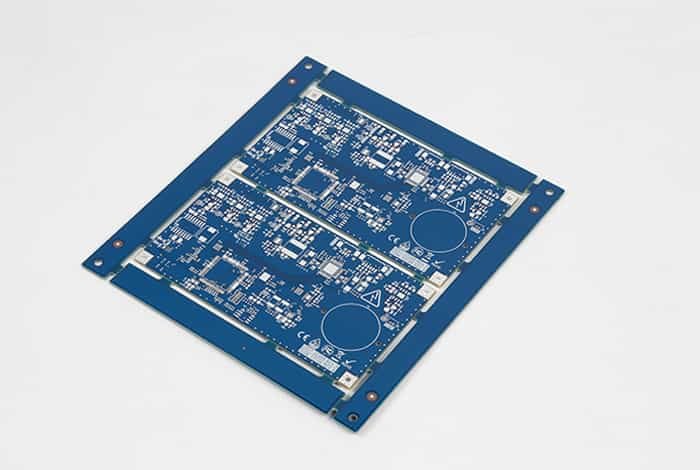
Blue Solder Mask
An alternative appearance for custom board projects. We coordinate the selected mask with the required finish, legend and manufacturing features rather than color alone.
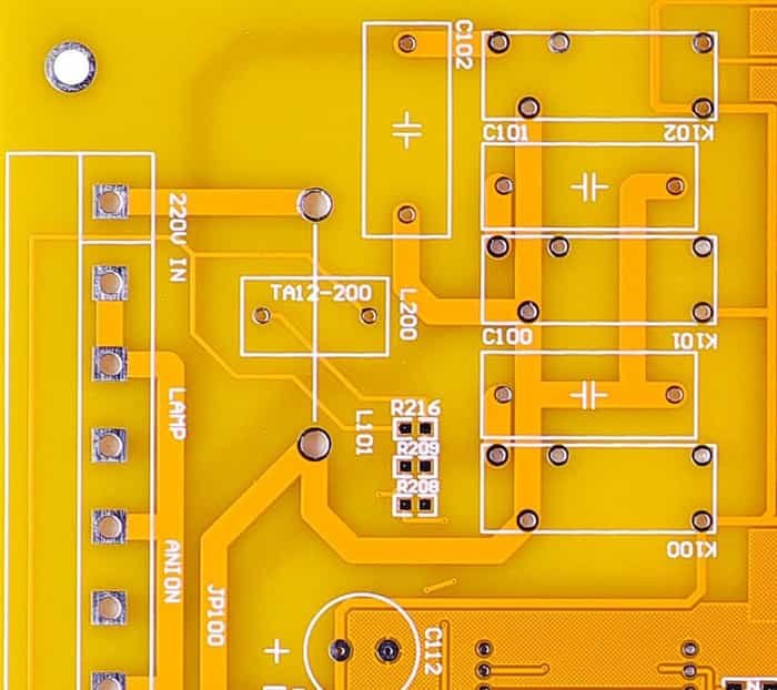
Yellow Solder Mask
A vivid option for a recognizable board appearance. Include the preferred legend color and identification requirements so the visual details are considered together.
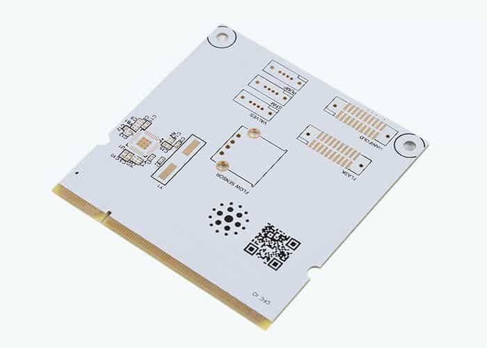
White Solder Mask
A useful option to discuss for LED PCB projects . Include any specified material, appearance or optical requirements with the board files for quotation.
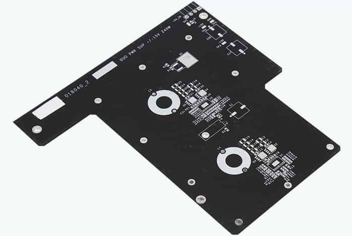
Black Solder Mask
Create a dark board appearance with contrasting identification. Tell us the desired matte or gloss appearance and marking requirements for the selected material system.
Color Is One Part of the Specification
The selected material, coverage, openings and finish all contribute to the manufactured board. Discuss them together with the PCB fabrication requirements of your project.
Include Controlled Appearance Requirements
If a color reference, material grade, surface appearance or acceptance sample is required, identify it with the manufacturing file package before production release.
Choose the Protection Around the Board Construction
Solder Mask Materials & Manufacturing Options
Solder mask is more than a color choice. PCBELEC helps coordinate the permanent mask, specified protection and material requirements with the complete PCB manufacturing build.
Swipe horizontally to view all material and protection options.
| Material / Protection Option | What It Does | Manufacturing Support |
|---|---|---|
| LPI Solder Mask Permanent liquid photoimageable system | A liquid-applied material patterned through imaging and development, then cured to form the permanent solder mask. | Color, coating coverage, pad openings, mask dams and registration coordinated with the artwork. |
| Specified Permanent Dry Film Film-based solder resist requirements | A permanent protective film system selected for the required board construction. It is distinct from temporary dry-film photoresist used in circuit processing. | Material-driven review of film specification, openings, processing and acceptance requirements. |
| Peelable Protection Temporary masking for specified regions | Temporary coverage for designated areas during selected downstream processes, removed when that protection is no longer needed. | Defined protection regions, process compatibility and removal requirements planned with the project. |
| Flexible-Circuit Coverlay A separate flexible protection construction | Protective film and bonding construction used in flexible circuit regions, with openings for required connection features. | Coverlay, openings, flexible materials and stiffeners coordinated through our flexible PCB manufacturing service. |
Have a specified material or approval requirement? Include it with the board files. Our team will help align the protection choice and manufacturing route.
Openings & Fine Features
Mask openings and dams need to work with the pad geometry. For dense layouts, our HDI manufacturing and BGA PCB fabrication services provide related engineering support.
Surface-Finish Coordination
Solder mask covers specified regions; surface finish serves the exposed circuit features. Review the PCB surface-finish guide when discussing the complete board.
Flexible Protection Choices
Coverlay and solder mask are not simply interchangeable labels. Our coverlay vs solder mask comparison explains the related flexible-circuit options.
Bring the Solder Mask Requirements into Your PCB Quote
Send the board files, quantity and preferred color. Add specified materials, protection regions or special requirements, and let our team help with the next step.
Precision Around the Pads and Circuit Features
Solder Mask Openings, Dams & Registration
Bring the mask artwork and copper geometry together before manufacturing. PCBELEC helps work through pad openings, mask bridges and alignment details so the finished board follows a clear fabrication specification.
A / Non-Solder-Mask-Defined Pad
NSMD: Copper Defines the Pad
The mask opening extends beyond the copper pad boundary. We review the opening and surrounding features with the copper artwork, registration allowance and project requirements.
B / Solder-Mask-Defined Pad
SMD: Mask Defines the Exposed Area
The mask overlaps the copper perimeter, leaving a smaller exposed area. Pad and opening dimensions are kept distinct during engineering review, particularly for specified package requirements.
The Details Behind a Manufacturable Mask
Swipe horizontally to view all engineering details.
| Feature | What It Describes | Manufacturing Support |
|---|---|---|
| Opening & Expansion | The mask opening and its relationship to the copper pad or other exposed feature. | Review of supplied mask artwork, copper boundaries and any proposed opening adjustments. |
| Dam / Web | The remaining mask bridge between adjacent openings, after the opening geometry has been established. | Feature review with material, color, imaging process and neighboring pad geometry. |
| Registration | Alignment of the mask pattern to the copper and required exposed regions. | Coordination of opening allowances, critical keepouts and acceptance requirements. |
| Coating Coverage & Thickness | The specified material coverage and thickness, with the relevant measurement locations identified. | Copper surfaces, edges and substrate regions considered with the selected material system. |
Keep Fine-Pitch Pad Requirements Clear
For dense pad patterns, coordinate the copper and mask together. Our BGA PCB fabrication and HDI manufacturing services provide related support for complex layouts.
Send the Copper and Mask Data Together
Include top and bottom mask layers with the corresponding circuit data. Use the PCB manufacturing file guide to prepare a matching release package.
Different Protection Choices, Clearly Defined
Via Protection & Special Solder Mask Requirements
Open, tented, plugged and filled vias describe different constructions. PCBELEC helps connect the intended protection, pad access and fabrication details with the complete board manufacturing requirements.
Open Via
The via remains open, with the pad and mask opening defined in the fabrication data. This is different from specifying a covered or filled hole.
Tented Via
Mask covers the specified hole opening. Tenting does not mean that the barrel is filled. Identify the required side and treatment with the board data.
Plugged Via
A specified plugging process places material into the via. Define the material, side and acceptance requirements rather than treating plugging as full fill or copper capping.
Filled & Capped Via
Filling and copper capping create a different construction from mask coverage. Learn more about filled and capped vias for related fabrication details.
Simplified cross-sections, not to scale. Materials, treatment sides and acceptance details follow the selected manufacturing construction.
White Mask & Lighting Requirements
White solder mask can form part of an LED PCB manufacturing project. We help coordinate the specified material, covered regions and appearance requirements with the board build.
- Material grade, color reference and critical coverage.
- Defined reflectance or aging requirements where controlled.
- Test conditions and acceptance criteria included with the specification.
Flexible Circuits & Coverlay
Flexible protection needs to work with the circuit's installation. Our flexible PCB service coordinates coverlay, connection openings and local reinforcement with the construction.
- Coverlay and opening geometry.
- Flexible regions, stiffeners and installation requirements.
- Related coverlay vs solder mask selection context.
Bring the Protection Details into the PCB Quote
Mark the required via treatment, special covered regions and material requirements with your board files. Our team can help coordinate the complete fabrication route.
Careful Preparation, Accurate Imaging & Finished-Board Checks
Solder Mask Process & Quality Control
A well-manufactured solder mask starts before the color is applied. PCBELEC brings surface preparation, material processing, imaging and inspection together as part of your complete PCB fabrication order.
Typical Liquid Photoimageable Solder Mask Process
-
01
Surface Preparation
Prepare the circuit surface for coating. Cleanliness and surface condition are addressed before the selected mask material is applied to the board.
-
02
Coating & Tack Drying
Apply the material through the selected coating process, then prepare it for imaging. Coverage and processing follow the requirements of the material system.
-
03
Imaging & Development
Define the mask pattern and develop the required openings. Pad access, mask bridges and registration remain key engineering and inspection features at this stage.
-
04
Final Cure & Inspection
Complete the material's final cure and inspect the mask condition. The board continues through the remaining fabrication and final inspection requirements.
Processing follows the selected material system. For additional context, review the solder mask, legend and surface-finish manufacturing stages .
Check More Than the Color
The finished appearance is only one part of the inspection. We connect coverage, openings and material requirements with the board's fabrication acceptance criteria.
Coverage & Appearance
Inspect the specified covered and exposed regions, board markings and visible mask condition against the released artwork and appearance requirements.
Openings & Registration
Review pad openings, remaining dams and alignment to copper. Critical features identified during engineering stay connected to the inspection focus.
Material & Specified Verification
Coating and cure follow the material requirements. Additional adhesion, thickness or other checks can be planned with the project specification.
Quality Requirements Planned with the Board
Need controlled appearance, measured thickness or supporting records? Include them with your inquiry. Our PCB testing and inspection resources provide related context for the complete order.
Bring the Mask Details into the Complete Board Build
Request a PCB Quote with Your Solder Mask Requirements
Send the board files and the requirements that matter to your project. PCBELEC helps coordinate the mask color, material, openings and protection details with custom bare PCB manufacturing.
What to Include
- Circuit artwork, top and bottom mask data, drill files and the finished outline.
- Board construction, quantity, materials and finished thickness where selected.
- Preferred mask color, specified material and controlled appearance requirements.
- Special openings, via treatment, protected regions and requested records.
- Required delivery date and destination.
Use our PCB manufacturing file guide to prepare a matching release package.
Still Comparing the Mask Options?
Tell us what is already decided and where you need support. Our team can help work through the material and fabrication details before production release.
Prefer to Send Your Files Directly?
sales@pcbelec.comPrepare Your PCB Fabrication Inquiry
Add the main board and mask requirements below. Review the generated email text, then add your files before sending.
If no email application opens, select and copy the text into your preferred email service. Add the files and send to sales@pcbelec.com.
Colors, Openings & Fabrication Questions
PCB Solder Mask FAQ
Practical answers to help you specify the mask, prepare the board files and discuss the next manufacturing step with PCBELEC.
What is solder mask, and is it the same as solder resist?
Solder mask, also called solder resist, is the protective material patterned over selected areas of the PCB surface. It covers specified circuit regions while leaving the required pads and connection features exposed. PCBELEC coordinates these details as part of the complete bare-board fabrication order.
What solder mask colors can I request?
Color options include green, red, blue, yellow, white and black. Share any specified material, matte or gloss appearance, color reference and legend requirements with the inquiry. See the solder mask color examples for the board images.
Does the color alone determine solder mask performance?
No. Color is one part of the specification. The material system, coating, imaging, cure and feature geometry also matter. We review controlled appearance or performance requirements with the selected material rather than treating each color as a fixed manufacturing or insulation grade.
How should I specify solder mask thickness?
Identify the required material, thickness acceptance criteria and relevant measurement locations. Coverage over copper, near copper edges and over substrate areas should be considered on the correct basis. Our team can help work through these requirements with the board construction.
See the process and quality-control section for the related inspection topics.
What is the difference between solder mask and paste mask?
Solder mask data defines the permanent mask pattern and its openings on the finished PCB. Paste-mask data defines openings used for solder paste printing, typically through a stencil. They serve different jobs and should not be treated as interchangeable fabrication layers.
Can you help review pad openings and solder mask dams?
Yes. We review the mask pattern with the copper artwork, including openings, remaining dams and registration requirements. The material and imaging route are considered alongside the pad geometry. See the openings, dams and registration section for the NSMD and SMD examples.
Is via tenting the same as plugging or filling?
No. Tenting covers a specified hole opening with mask; it does not mean that the barrel is filled. Plugging, full filling and copper capping describe different constructions. Identify the intended treatment and sides with the manufacturing data.
Compare the via-protection illustrations before defining the requirement.
Can flexible PCBs use the same protection as rigid boards?
Flexible regions need protection coordinated with their material and installation requirements. Coverlay is a separate protective construction, not simply another name for rigid-board solder mask. Our flexible PCB manufacturing service supports coverlay, openings and local reinforcement requirements.
Can I request white mask with reflectance or aging requirements?
Include the required material specification, covered regions, test conditions and acceptance criteria with the inquiry. We can review these requirements alongside the complete LED PCB manufacturing project. White color alone is not a defined reflectance or non-yellowing specification.
What files should I send for a PCB quote with special mask requirements?
Send the circuit artwork, mask layers, drill data, finished outline and quantity. Add the preferred color, specified material, special openings, via treatment and any controlled appearance or inspection requirements. Use our PCB manufacturing file guide to prepare one matching release package.
Where should I request component sourcing and PCB assembly?
This PCBELEC page supports bare-board manufacturing inquiries with specified solder mask requirements. For component sourcing and PCB assembly, continue to PCB assembly services at JHYPCB and discuss the populated-board project through that service.
Have a project-specific mask requirement? Include it with your PCB fabrication inquiry and let our team help with the next manufacturing step.
Related Manufacturing & Technical References
Solder Mask & PCB Fabrication Resources
Find more detail on manufacturing preparation, via protection and the board services connected to your solder mask requirements.