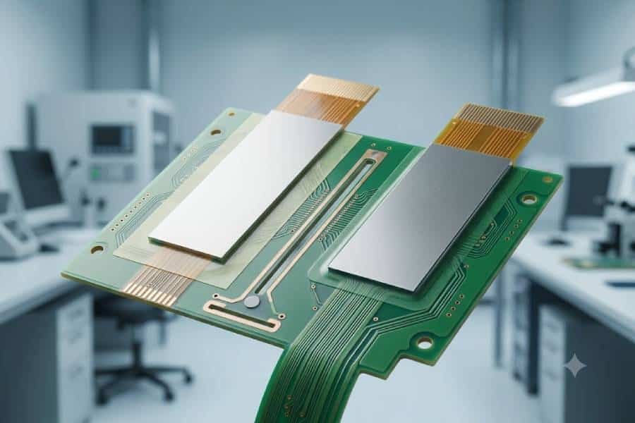
Multilayer Flexible PCB Manufacturer – Custom 4–16 Layer Flex Circuits
Lightweight, high‑density multilayer flexible PCBs for compact, reliable electronics in consumer, automotive, medical, and industrial applications.
- Up to 16‑layer multilayer flex and rigid‑flex PCB manufacturing.
- 10+ years flex PCB experience in China, 1M+ flex circuits shipped per year.
- Polyimide‑based flex circuits with ENIG, hard gold and other finishes for high‑reliability interconnects.
- Tight tolerances on fine lines, microvias and controlled impedance for high‑speed designs.
- Quick‑turn multilayer flex PCB prototyping and volume production from China.
Get a Multilayer Flex PCB Quote Today
Upload your Gerber and requirements, our engineers will review your multilayer flex PCB design and send a detailed quote within 24 hours.
Multilayer Flex PCB Capabilities
Our multilayer flexible PCB capabilities support high‑density, high‑reliability designs for demanding applications. The table below shows our standard manufacturing range; please contact us if you need tighter or special requirements.
Multilayer flexible circuits combine several conductive layers to achieve higher routing density, better signal integrity, and more complex interconnections than single‑ or double‑sided flex PCBs.
We manufacture multilayer flex PCBs and rigid‑flex boards with stable quality and strict process control to meet the needs of compact and mission‑critical electronics.
- Standard multilayer flex up to 16 layers, higher layer counts on request after engineering review.
- DFM support for stack‑up, bend radius and impedance planning before production.
Key Multilayer Flex PCB Manufacturing Capabilities
| Capability | Standard Range |
|---|---|
| Layer count | 3–16‑layer multilayer flex circuits; higher counts evaluated case‑by‑case. |
| Base material | Polyimide (PI) adhesive and adhesiveless flex laminates; PET available for selected low‑cost applications. |
| Copper thickness | 1/3 oz to 2 oz standard; up to 4–6 oz available on request. |
| Min. trace / space | Typically down to 0.075 / 0.075 mm (3 / 3 mil); finer features subject to review. |
| Min. finished hole | 0.20 mm (8 mil) mechanical via; laser microvias available for HDI flex designs. |
| Finished thickness | Approx. 0.05–2.5 mm depending on stack‑up, copper weight and stiffeners. |
| Max panel size | Typical panel up to around 250 × 400 mm; larger sizes can be discussed. |
| Surface finishes | ENIG, immersion gold, hard gold (selective / gold fingers), immersion tin, OSP and others. |
| Stiffeners | Polyimide, FR‑4 and stainless / aluminum stiffeners for connector and mechanical support areas. |
| Impedance control | Differential and single‑ended controlled impedance with typical ±10% tolerance. |
What Is a Multilayer Flexible PCB?
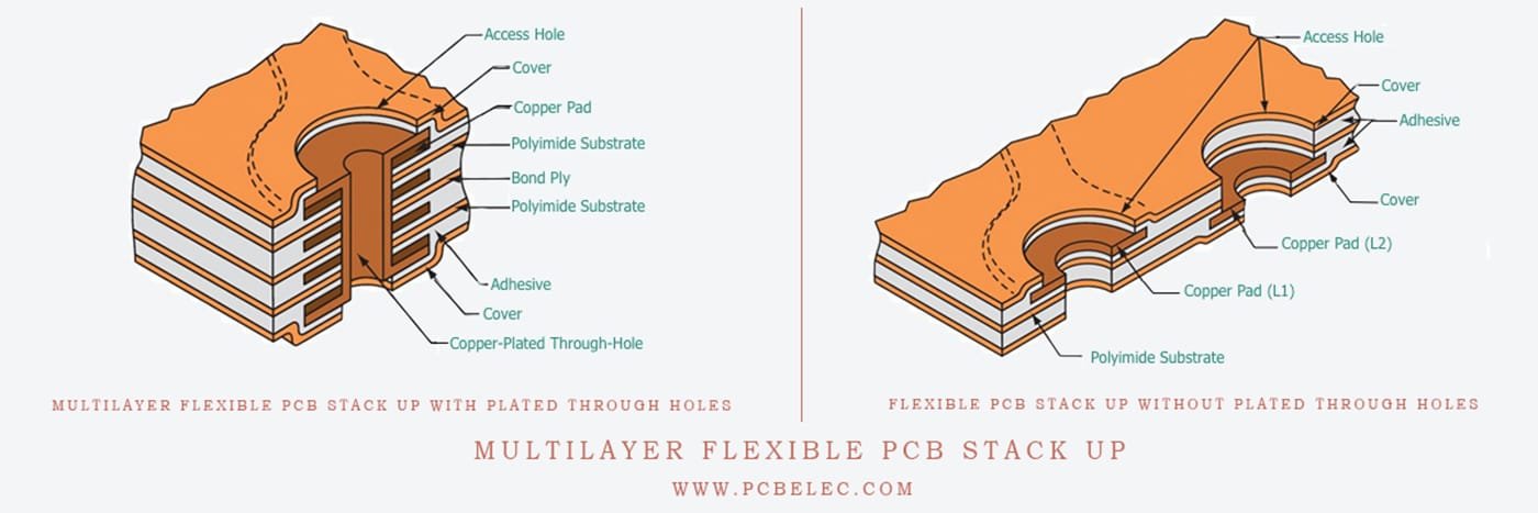
A multilayer flexible PCB is a flex circuit that combines three or more copper layers with polyimide insulation and plated‑through holes to create complex, high‑density interconnections in a bendable format.
Compared to simple single‑ or double‑sided flex, multilayer flex circuits can route more signals in a smaller area, integrate power and ground planes, and support controlled impedance for high‑speed designs.
By replacing bulky wire harnesses and connectors, multilayer flexible PCBs reduce weight and thickness while improving reliability, signal integrity and assembly efficiency.
They are widely used in compact, mission‑critical electronics such as portable medical devices, automotive electronics, industrial controls, and consumer products where space, performance and reliability are all critical.
Single‑, Double‑ and Multilayer Flex PCBs at a Glance
| Type | Structure & Features | Typical Use Cases |
|---|---|---|
| Single‑layer flex | One copper layer on a polyimide base with coverlay, highest flexibility, lowest cost but limited routing density. | Simple interconnects, dynamic flex cables, printers, scanners, low‑complexity consumer devices. |
| Double‑layer flex | Two copper layers with plated‑through holes and polyimide insulation, higher circuit density and more routing options while still very flexible. | Slightly more complex interconnects, fine‑pitch connectors, moderate‑speed signals in consumer, automotive and industrial products. |
| Multilayer flex | Three or more copper layers laminated together with PI insulation and PTHs, can integrate ground/power planes, shielding and dense SMT areas, but bending radius is larger than single / double flex. | High‑density, high‑speed and space‑constrained designs in medical, automotive, aerospace, industrial and advanced consumer electronics. |
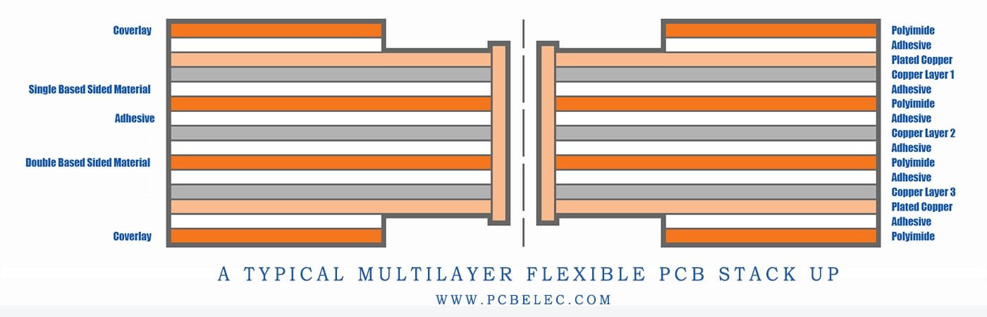
Multilayer Flex PCB Stack‑Up & Design Guidelines
A well‑planned stack‑up is critical to achieving the right balance between flexibility, reliability and electrical performance in multilayer flex PCBs.
Our engineers can help you optimize layer structure, bend areas and impedance so your design is manufacturable and robust from prototype to volume production.
Typical Multilayer Flex Stack‑Ups
The following examples show common stack‑ups for 4‑layer and 6‑layer flexible circuits; actual constructions are customized based on your impedance, thickness and bending requirements.
4‑Layer Multilayer Flex (Example)
- Top coverlay
- Copper layer 1 – signal
- Polyimide dielectric
- Copper layer 2 – ground plane
- Polyimide dielectric
- Copper layer 3 – power / signal
- Polyimide dielectric
- Copper layer 4 – signal
- Bottom coverlay
This 4‑layer stack‑up uses an internal ground plane and optional power plane to improve signal integrity and reduce EMI while keeping overall thickness suitable for controlled, limited bending.
6‑Layer Multilayer Flex (Example)
- Top coverlay
- Copper layer 1 – high‑speed signal
- Polyimide dielectric
- Copper layer 2 – ground plane
- Polyimide dielectric
- Copper layer 3 – inner signal / power
- Polyimide dielectric
- Copper layer 4 – inner signal / power
- Polyimide dielectric
- Copper layer 5 – ground plane
- Polyimide dielectric
- Copper layer 6 – signal / pads
- Bottom coverlay
A 6‑layer stack‑up allows separate reference planes for high‑speed signals and more routing channels, ideal for dense connectors and mixed‑signal designs where impedance control and noise isolation are critical.
Unbonded multilayer flex constructions are also available for applications that require higher dynamic bending performance and thinner overall thickness.
Bend Radius and Flexibility Considerations
As multilayer flex circuits become thicker, the minimum bend radius increases and dynamic bending becomes more limited, especially compared to single‑layer or double‑layer flex.
IPC‑2223 guidelines and industry practice generally recommend much larger bend radii for multilayer flex, and in many cases dynamic, continuously flexing designs are better kept to two layers or fewer.
- Try to keep flex thickness as low as practical in bend areas by reducing copper weight and avoiding unnecessary stiffeners.
- For static bends, a minimum bend radius of roughly 15–20× the total flex thickness is often used as an initial guideline for multilayer flex circuits.
- Avoid placing vias, pads and sharp trace corners in bend regions; route traces perpendicular to the bend with smooth arcs instead of 90‑degree angles.
- Use rolled‑annealed (RA) copper rather than ED copper in any area that will bend repeatedly to reduce the risk of cracking.
Layer Assignment and Routing Best Practices
Proper layer assignment helps maintain signal integrity and mechanical reliability while keeping the stack‑up cost‑effective.
- Reserve at least one solid ground plane close to your high‑speed layers to provide stable impedance and reduce crosstalk.
- Place sensitive analog or RF traces away from noisy digital or power layers, and avoid routing high‑speed signals over split planes.
- Concentrate most vias and dense SMT components in relatively stiff, low‑strain areas; keep flexing regions as simple and uniform as possible.
- Document your intended stack‑up and flex / rigid zones clearly in the fabrication drawing so manufacturing matches your design intent.
If you share your target thickness, bend requirements and impedance constraints, our team can propose a custom multilayer flex stack‑up and DFM recommendations before you start layout.
Materials, Surface Finishes and Stiffeners for Multilayer Flex PCBs
Choosing the right base material, surface finish and stiffener configuration is essential to achieving the desired flexibility, reliability and assembly performance of multilayer flex PCBs.
We work primarily with high‑performance polyimide laminates, proven surface finishes and a range of stiffener options to match your electrical, mechanical and cost targets.
Base Materials & Coverlay
Polyimide is the most widely used substrate for multilayer flexible PCBs because it combines excellent bend life, thermal stability and electrical performance.
For special low‑cost or transparent applications, PET and other polymer films can also be used when temperature and reliability requirements allow.
- Polyimide (PI) flex laminates – standard choice for multilayer flex circuits, offering high temperature resistance, good dielectric properties and long bend life.
- Adhesiveless PI – improved flexibility, thinner stack‑ups and better dimensional stability for tight bend areas and fine‑pitch designs.
- PET and other films – optional for cost‑sensitive or transparent flex circuits operating at lower temperatures and moderate bend requirements.
- PI coverlay – robust protection for copper traces in the flex area, providing insulation and resistance to mechanical and environmental stress.
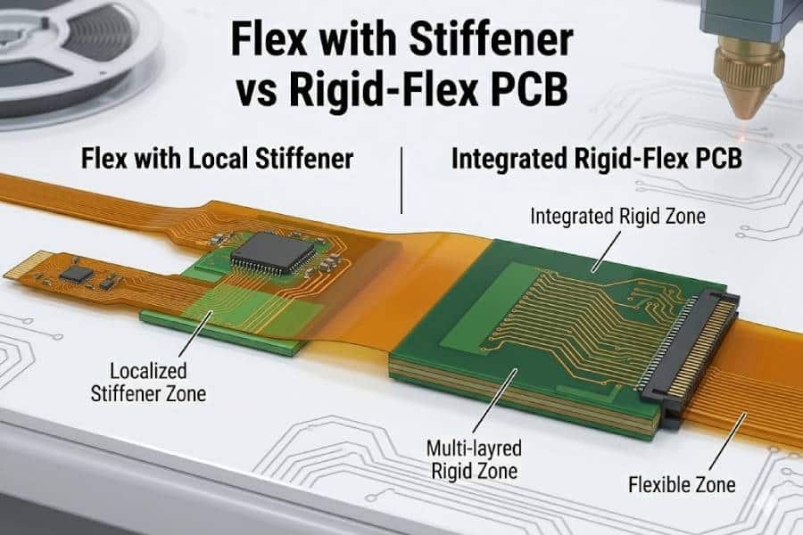
Stiffeners for Connectors and Component Areas
Local stiffeners are used to reinforce connector and component areas so that solder joints are protected and the flex circuit handles more like a rigid PCB where needed.
By combining flexible zones with polyimide, FR‑4 or metal stiffeners, multilayer flex PCBs can meet both mechanical strength and bending requirements.
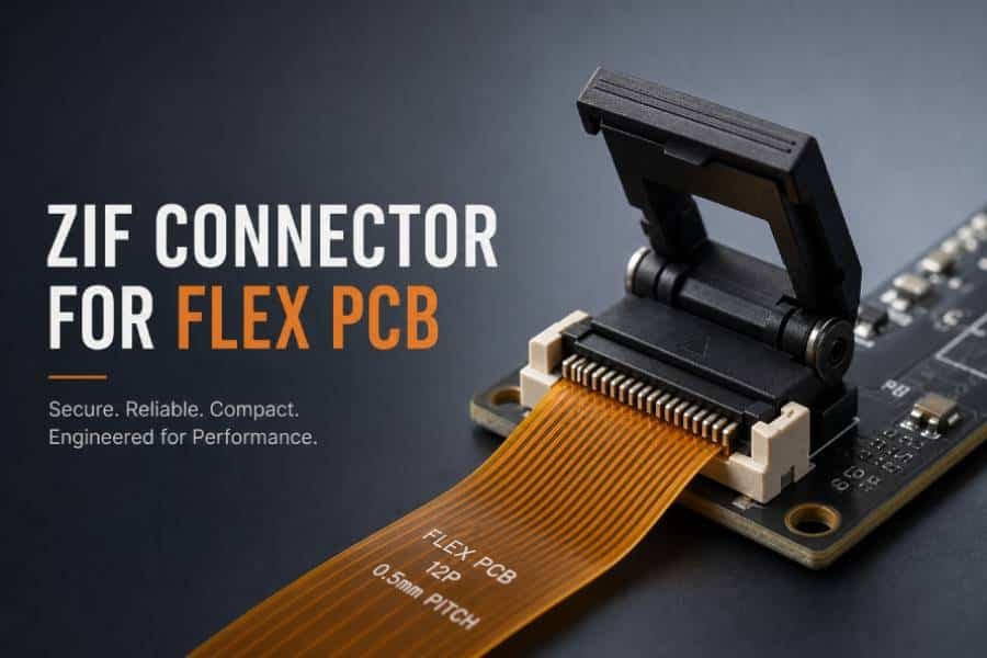
- Polyimide stiffeners – ideal for ZIF contacts and areas where precise thickness and tight outline tolerances are required.
- FR‑4 stiffeners – commonly used under connectors and larger components to prevent bending at solder joints and to improve handling during assembly.
- Stainless steel / aluminum stiffeners – used when additional rigidity or heat spreading is needed in high‑power or mechanically stressed areas.
We can recommend suitable stiffener materials and thicknesses based on your connector requirements, component layout and target overall thickness.
Surface Finishes for Multilayer Flex PCBs
| Surface finish | Typical use and benefits |
|---|---|
| ENIG (Electroless Nickel Immersion Gold) | Flat, solderable finish ideal for fine‑pitch SMT, BGAs and via‑in‑pad designs; good corrosion resistance and widely used on multilayer flex PCBs. |
| Hard gold (electrolytic) | Very wear‑resistant finish for edge connectors and gold fingers that see repeated mating cycles; usually used selectively due to higher cost and lower solderability in large areas. |
| Soft gold (wire‑bondable) | Suitable for wire‑bond pads and special high‑reliability contact areas where low contact resistance is critical. |
| Immersion tin / OSP | Cost‑effective finishes for solderable areas when gold fingers or wire bonding are not required, often used on more price‑sensitive multilayer flex designs. |
Applications of Multilayer Flexible PCBs
Multilayer flex PCBs are used wherever compact, high‑density and reliable interconnections are needed in space‑constrained or moving electronics.
They replace bulky wire harnesses and rigid boards in many consumer, automotive, medical, industrial and aerospace systems to save space, reduce weight and improve reliability.
Key Industries Using Multilayer Flex PCBs
| Industry | Typical applications | How multilayer flex PCBs help |
|---|---|---|
| Consumer electronics | Smartphones, tablets, cameras, foldable devices, wearables, AR/VR headsets. | Connect displays, cameras, batteries and sensors in very thin housings, enabling 3D packaging and hinge designs while reducing weight and connector count. |
| Automotive electronics | Instrument clusters, infotainment, ADAS modules, sensors, lighting systems, EV battery and power control. | Withstand vibration and temperature changes while routing dense signals in tight spaces, replacing wire harnesses and improving reliability and assembly efficiency. |
| Medical devices & wearables | Portable diagnostics, patient monitors, imaging probes, hearing‑assist devices, implantable and wearable health trackers. | Enable ultra‑compact, lightweight and conformable electronics that fit the human body or tight instrument channels with high reliability and reduced interconnect failures. |
| Industrial & robotics | Factory automation, sensors, motion controllers, robots, measurement and test equipment. | Provide durable interconnections that tolerate vibration, repeated movement and harsh environments while simplifying assembly and maintenance. |
| Aerospace & defense | Avionics, communication modules, satellites, radar and guidance systems. | Reduce weight and volume, improve shock and vibration performance, and support high‑reliability interconnects in mission‑critical systems. |
If you share your target industry and application, we can recommend suitable multilayer flex PCB stack‑ups, materials and surface finishes tailored to your reliability and cost requirements.
Our engineering team regularly supports projects ranging from high‑volume consumer electronics to low‑volume, high‑reliability medical and aerospace systems.
Multilayer Flex PCB Quote and Ordering Process
Getting a multilayer flex PCB quote is straightforward – just share your design files and basic requirements, and our engineers will review them and provide detailed pricing and lead times.
We support both quick‑turn prototypes and volume production, with engineering feedback to help you optimize cost and manufacturability.
How to Order Multilayer Flexible PCBs from JHYPCB
Ready to start your multilayer flex PCB project? Upload your design files or contact our team, and we will respond with a customized quote and DFM feedback within 24 hours on working days.
Multilayer Flex PCB FAQ
Here are answers to some of the most common questions engineers and buyers ask about multilayer flexible PCB design and manufacturing.
How many layers can you manufacture for multilayer flex PCBs?
What is the typical lead time for multilayer flex PCB prototypes and production?
What is your minimum order quantity (MOQ) for multilayer flexible PCBs?
What design files do you need to quote and manufacture multilayer flex PCBs?
How to Change my Photo from Admin Dashboard?
Can you help review my multilayer flex PCB design for manufacturability (DFM)?
When should I choose multilayer flex vs. rigid‑flex?
If your question is not listed here, please contact us with your multilayer flex PCB requirements and our team will respond with detailed answers and design suggestions.