


Double Sided PCB Manufacturing
High-quality double-sided PCB prototyping and production tailored to your needs. Fast delivery, free DFM, and 15+ years of expertise. Start your project today!
Why Choose JHYPCB for Double Sided PCBs?
As a trusted PCB manufacturer in China, JHYPCB specializes in high-quality double-layer PCB solutions. With over 15 years of experience, we deliver boards tailored to your needs, from prototypes to mass production.
Double Sided PCB Definition
What is a Double Sided PCB?
A double-sided PCB, also known as a double-layer PCB or 2-layer PCB, features conductive copper layers on both sides of a substrate, typically FR4. This design enables components and circuits on both top and bottom layers, connected via plated-through holes (vias) for enhanced functionality.
Key Features
- Higher Component Density: Supports compact designs for devices like mobile phones and IoT gadgets.
- Flexible Routing: Vias enable complex circuit connections, unlike single-sided PCBs.
- Wide Applications: Ideal for LED lighting, automotive dashboards, and RF systems.
At JHYPCB, we deliver high-quality double-sided PCB manufacturing. Get a free quote today!
double sided circuit boards
Types of double-sided PCB
JHYPCB manufactures various double sided PCB types to suit diverse applications:
- Rigid PCB: FR4 substrate for consumer electronics like LED lighting.
- Flexible PCB: Polyimide material for wearables.
- Metal Core PCB: Aluminum core for heat dissipation in high-power LEDs.
- High Tg PCB: Thermal stability for industrial controls.
- High Frequency PCB: Rogers material for RF and microwave circuits.
- Heavy Copper PCB: Thick copper for power electronics.
- Impedance Control PCB: Ensures signal integrity for high-speed circuits.
Need a custom double-layer PCB? Request a quote today!
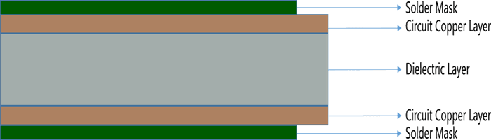
Double Sided PCB Stack-Up
Understanding the stack-up is crucial for effective double sided PCB design. JHYPCB ensures precision in every layer:
Core Layers
- Top Conductive Layer: Copper for conductivity; gold/silver for plating.
- Dielectric/Base Layer: FR4, Polyimide, or PTFE as an insulator.
- Bottom Conductive Layer: Mirrors top layer for dual-sided circuits.
Protective Layers
- Surface Finish: OSP, Immersion Gold, or Tin to prevent oxidation.
- Solder Mask: Prevents solder bridges.
- Silkscreen: Labels components for assembly.
Optimize your design with JHYPCB’s expertise. Get started!
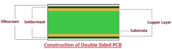
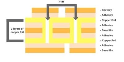
Construction of double-sided PCB
Double Sided PCB Layers
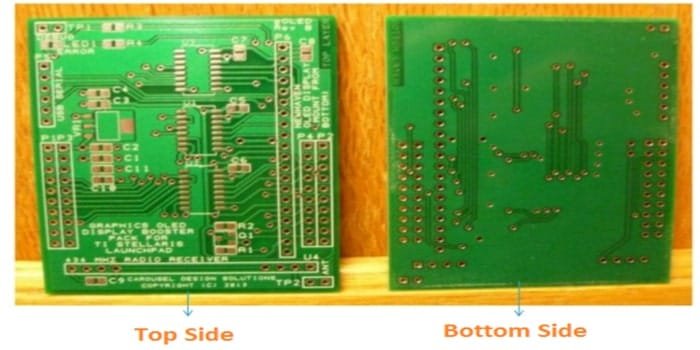
Double Sided PCB-Top Side and Button Side
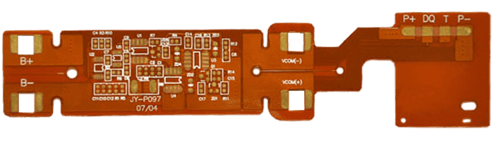
Double-sided Flexible PCB Circuit Board
Double-sided Flexible PCB Stack-up
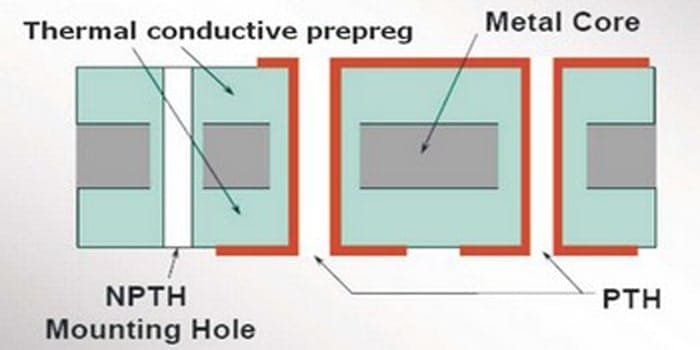
Structure of Double Sided MCPCB
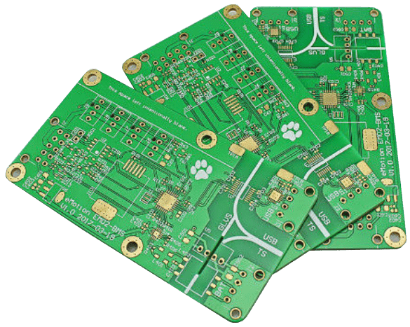
Double Layer PCB Prototype Manufacturer
Benefits of Double Sided PCBs
Double sided PCBs offer significant advantages for modern electronics:
- Increased Component Density: Double the space for compact designs.
- Flexible Routing: Vias and dual layers reduce congestion.
- Better Signal Integrity: Ground plane minimizes noise.
- Space-Saving: Half the size of single-sided PCBs.
- Cost-Effective: Affordable alternative to multilayer PCBs.
Leverage these benefits with JHYPCB’s double layer PCB solutions. Request a quote now!
Double Sided PCB Prototyping
JHYPCB offers rapid double sided PCB prototype fabrication for applications like LED systems, wearables, and RF circuits.
Prototype Options
- Material Choices: FR4, metal-core, or flexible polyimide.
- Surface Finishes: Immersion Gold, OSP, Lead-Free Tin.
- Quick-Turn: 24-hour delivery for prototypes.
Start your double layer PCB project with us. Get a free quote today!
Double-Sided PCB Fabrication Capabilities
JHYPCB is a trusted double-sided PCB manufacturer in China, specializing in quick-turn prototyping and mass production. With over 15 years of experience, we deliver high-quality boards tailored to your needs. Explore our fabrication capabilities:
Key Fabrication Specifications
| Parameter | Details |
|---|---|
| Materials | FR4, Copper Core, Aluminum, Rogers (for high-frequency applications) |
| PCB Size | Up to 680mm x 1200mm |
| PCB Thickness | 0.2mm to 6.0mm (customizable) |
| Surface Finishes | OSP, Immersion Silver/Gold/Tin, Plated Gold, Flash Gold |
| Solder Mask | Green, Red, White, Black, Blue, Yellow |
Supported PCB Types
- Double-Sided FR4 PCB: Standard for consumer electronics.
- Double-Sided Copper-Clad PCB: High conductivity for power applications.
- Double-Sided Flexible PCB: Ideal for wearable devices.
- Double-Sided Rigid-Flex PCB: Combines flexibility and rigidity for complex designs.
- Double-Sided Rogers PCB: Perfect for RF and microwave circuits.
JHYPCB offers 24-hour quick-turn prototyping and free DFM analysis to ensure precision. Need a custom double-sided PCB? Request a quote today!
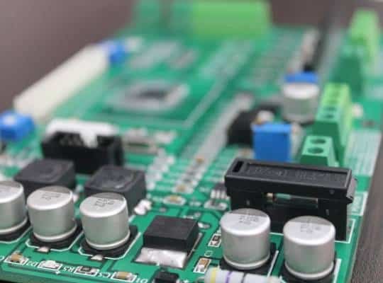
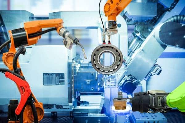
Double Sided PCB Assembly Process
Our double-sided PCB assembly uses advanced SMT and THT technologies for precision and reliability.
Assembly Steps
- Solder Paste Printing: Apply paste to both sides.
- Pick and Place: Place components accurately.
- Soldering: Reflow soldering for secure connections.
- Inspection: Ensure quality with visual and automated checks.
Need double-sided PCB assembly? Contact us for turnkey solutions!
Double Sided PCB Manufacturing Process
JHYPCB’s rigorous double sided PCB manufacturing process ensures quality and performance:
STEP 1
DFM Check
DFM Check
Verify design for manufacturability.
STEP 2
Drilling & PTH
Drilling & PTH
Create vias for layer connectivity.
STEP 3
Plating & Etching
Plating & Etching
Apply copper and remove excess.
STEP 4
Surface Finish & Testing
Surface Finish & Testing
Apply finishes and perform E-tests.
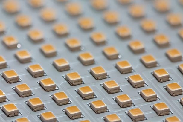
Applications of Double Sided PCBs
Double sided PCBs are versatile for industries including:

Consumer Electronics
Mobile phones, LED lighting
Power Applications
Inverters, UPS systems
Industrial Systems
HVAC, industrial controls

Automotive
Dashboards, sensors
Explore our solutions for your industry. Get a quote!
Frequently Asked Questions
What is the difference between single-sided and double-sided PCBs?
How long does it take to fabricate a double-sided PCB prototype?
What surface finishes are available?
Is there a minimum order quantity?
Recommended PCB Manufacturing Services


Related Posts
- Custom Circuit Board Printing
- Custom PCB Manufacturer In China
- Best PCB Manufacturer In China
- How To Search for a Reliable PCB Manufacturer
- PCB and PCBA Manufacturing Files
- Find Out Now, What Should You Do For Fast PCB Classification?
- What is a Multilayer PCB, and What Are the Advantages?
- Single-layer PCB vs. Double-sided PCB: How to Choose?
- How to Store PCB and PCBA?
- The Benefits Of Using Double Sided PCBs