Introduction
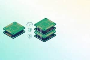
When designing PCBs, engineers face critical decisions about layout and component placement to balance functionality and manufacturability. One pivotal choice is opting for single-sided or double-sided PCBs. While single-sided boards are simpler and cheaper, they limit design complexity. Double-sided PCBs, with conductive layers on both sides, unlock greater flexibility and performance, making them ideal for prototyping. This article explores four key benefits of double-sided PCBs: increased layout space, support for complex circuits, improved signal integrity, and flexible component placement. Discover why JHYPCB’s double-sided PCB manufacturing and assembly services are perfect for your next project.
Table of Contents

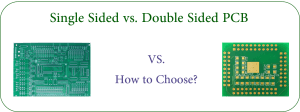
What Are Double-Sided PCBs?
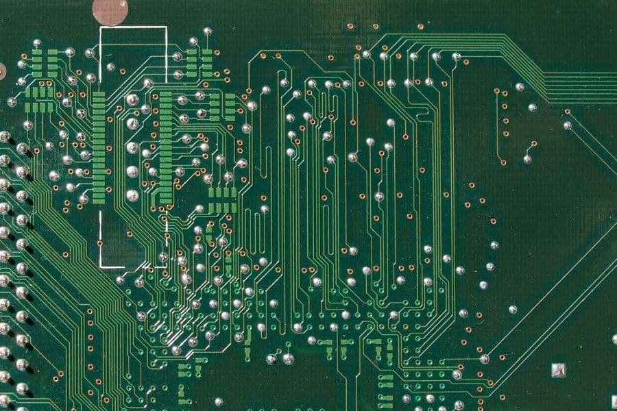
Double-sided PCBs feature conductive copper layers on both sides of a non-conductive substrate, connected via plated-through holes (vias). Unlike single-sided PCBs, which have only one conductive layer, double-sided boards offer more space for traces and components, enabling intricate designs. At JHYPCB, we specialize in manufacturing high-quality double-sided PCBs for prototyping and low-volume production, ensuring precision and fast turnaround. Contact us at sales@pcbjhy.com to learn more.
Key Benefits of Double-Sided PCBs
1. Increased Layout Space
Double-sided PCBs provide twice the real estate for traces, components, and vias compared to single-sided boards. This added space alleviates the constraints of single-layer designs, where engineers struggle to align components while maintaining trace spacing. With dual layers, you can:
- Host more components, including ICs, passives, and connectors.
- Route complex signal paths without compromising layout.
- Incorporate copper fills and text markings for clarity.
For example, a microcontroller-based project with multiple peripherals can be efficiently laid out on a double-sided PCB, reducing design compromises. JHYPCB’s precision manufacturing ensures your layout is realized with high accuracy.

2. Support for Complex Circuits
Double-sided PCBs enable intricate circuit designs with just two layers, minimizing costs and lead times for prototyping. Single-sided boards often require suboptimal routing to connect distant components, leading to cluttered layouts. In contrast, double-sided boards allow:
- Strategic placement of functional blocks (e.g., microcontrollers, power regulators) for shorter trace paths.
- Efficient use of vias to connect top and bottom layers.
- Reduced layer counts compared to multi-layer alternatives (e.g., 4 or 6 layers).
This makes double-sided PCBs ideal for testing ambitious designs, such as IoT devices or wireless modules, without excessive complexity. JHYPCB’s assembly services, including SMT and THT, streamline your prototyping process.

3. Enhanced Signal Integrity
Signal integrity is critical for high-speed digital or sensitive analog circuits. Long traces on single-sided PCBs increase parasitic resistance and capacitance, risking signal degradation. Double-sided PCBs address this by:
- Shortening trace lengths with direct top-to-bottom routing.
- Incorporating ground planes for better shielding and noise reduction.
- Isolating sensitive signals (e.g., clock lines or RF paths) from interference.
For instance, a radio tuner circuit benefits from shorter, shielded traces on a double-sided PCB, ensuring clean signals. JHYPCB’s high-quality fabrication enhances signal performance for reliable prototypes.
4. Flexible Component Placement
Double-sided PCBs offer unmatched flexibility in arranging components and routing traces. Engineers can:
- Position related components (e.g., decoupling capacitors near ICs) for optimal performance.
- Use one layer for critical nets to avoid obstructions.
- Leverage automated or manual routing for efficient layouts.
This versatility transforms complex designs into reality, enabling rapid iteration. For example, a sensor module with analog and digital components can be organized efficiently on a double-sided PCB. JHYPCB’s expertise in PCB assembly ensures your design is built to spec.
Why Double-Sided PCBs Are Ideal for Prototyping
Double-sided PCBs strike a balance of affordability, performance, and flexibility, making them perfect for prototyping. They allow engineers to test innovative circuits quickly without the high costs of multi-layer boards. Benefits include:
- Cost-Effective: Fewer layers reduce fabrication costs.
- Fast Turnaround: Simplified designs speed up production.
- Creative Freedom: Dual layers enable complex, functional prototypes.
Whether you’re developing digital circuits, analog sensors, or power controllers, double-sided PCBs accelerate validation. JHYPCB’s tailored solutions support your prototyping goals with precision and speed.
Partnering with JHYPCB for Double-Sided PCB Solutions
At JHYPCB, we specialize in delivering high-quality double-sided PCBs and assembly services for prototyping and low-volume production. Our offerings include:
- PCB Manufacturing: Precision fabrication of double-sided, rigid, flexible, and rigid-flex PCBs.
- PCB Assembly: SMT, THT, and turnkey assembly with component sourcing and SMT stencil services.
- Fast Delivery: Expedited lead times to meet tight project deadlines.
Contact us at sales@pcbjhy.com to discuss your project and discover how JHYPCB can bring your designs to life with affordable, high-performance solutions.
Conclusion
Double-sided PCBs offer significant advantages for prototyping, including increased layout space, support for complex circuits, enhanced signal integrity, and flexible component placement. These benefits empower engineers to create innovative, functional designs efficiently. JHYPCB’s expertise in PCB manufacturing and assembly ensures your prototypes are built with precision and delivered on time. Ready to start your next project? Reach out to JHYPCB at sales@pcbjhy.com for top-quality double-sided PCB solutions.
FAQs
What is the cost of double-sided PCBs?
Costs vary based on design complexity and order volume. Contact JHYPCB at sales@pcbjhy.com for a custom quote tailored to your project.
How fast can JHYPCB deliver double-sided PCB prototypes?
JHYPCB offers expedited manufacturing and assembly, often delivering prototypes in as little as 3-5 days. Email us for details.
Can double-sided PCBs support high-frequency circuits?
Yes, double-sided PCBs enhance signal integrity for high-frequency circuits with shorter traces and ground planes, ideal for RF and digital designs.