


Table of Contents
Why Stencils Matter in SMT Assembly
In Surface Mount Technology (SMT) assembly, stencils are critical for applying solder paste with precision, directly influencing PCB quality and reliability. A well-designed stencil ensures uniform paste deposition, enabling accurate component placement and minimizing defects like solder bridging or insufficient solder. Choosing the right stencil type—such as laser cut or etching stencils—impacts production efficiency, yield rates, and overall costs. At JHYPCB, a leading PCB manufacturer in China, we understand the stakes. Our expertise in stencil manufacturing and PCB assembly services helps clients achieve optimal results. This guide compares laser cut vs. etching stencils, exploring their precision, cost, and applications to help you select the best solution for your PCB projects. Whether you’re prototyping or scaling production, understanding stencil technology is key to success.
Laser Cut Stencils: Precision and Performance in SMT Assembly
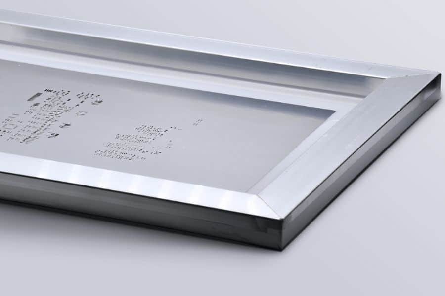
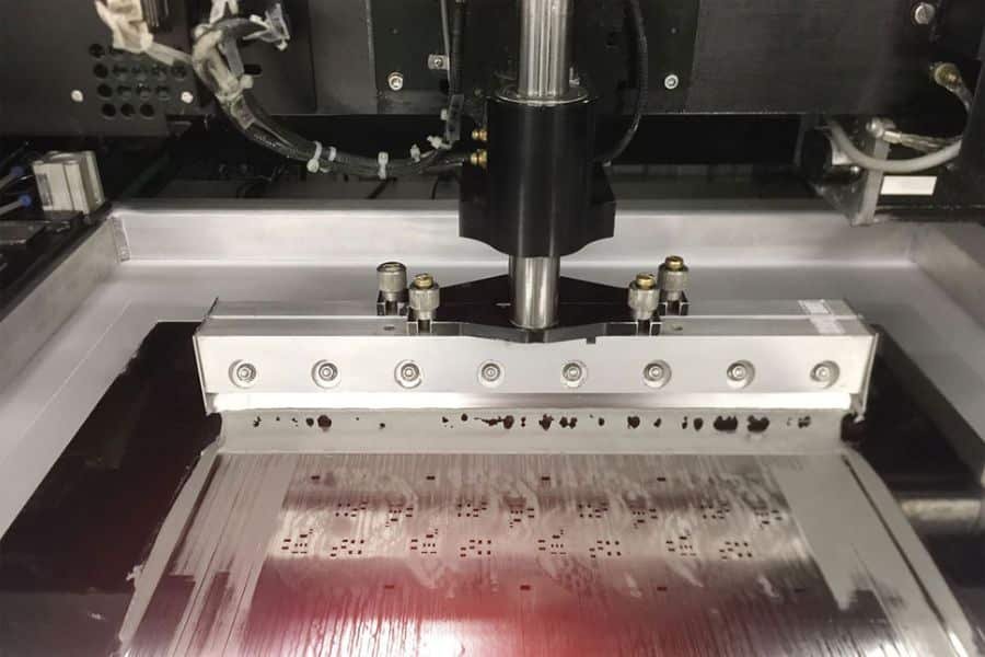
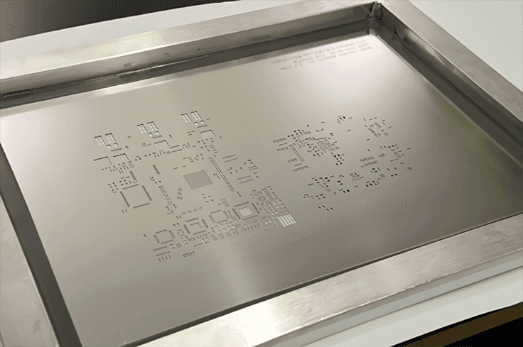
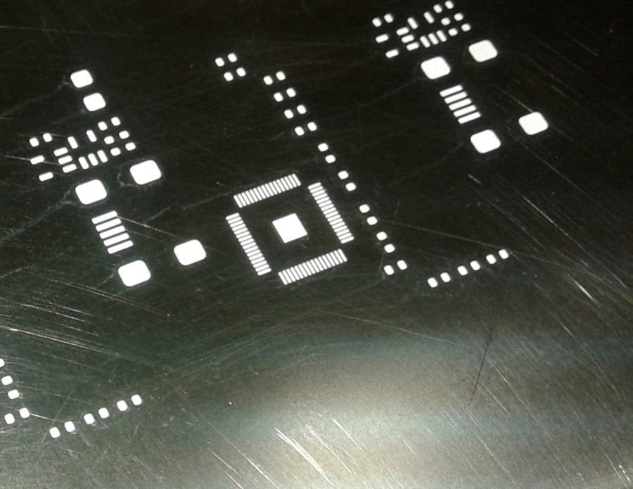
To make an informed choice, let’s first explore laser cut stencils, the industry standard for modern SMT assembly. These stencils are crafted using high-precision laser machines that carve apertures into stainless steel sheets with tolerances as tight as ±5-10 µm. The computer-controlled process ensures repeatability, making them ideal for fine-pitch components like QFPs, BGAs, and 0201/01005 packages. The smooth, trapezoidal aperture walls promote consistent solder paste release, reducing defects such as solder bridging or insufficient paste.
Key advantages include rapid production—often same-day or next-day—supporting rapid PCB prototyping. Laser cut stencils also excel in complex designs, accommodating step stencils or variable aperture sizes for mixed-technology PCBs. At JHYPCB, our advanced laser cutting technology ensures high-quality stencils tailored to your PCB assembly needs. However, laser cut stencils may have higher costs for intricate designs, and material options are limited to stainless steel or compatible alloys. For high-density, high-reliability PCBs, their precision and performance make them a top choice in stencil manufacturing.
Etching Stencils: Cost-Effective Solutions for SMT Assembly
In contrast, etching stencils, also known as chemically etched stencils, offer a different approach. They are produced by applying a chemical etching process to metal sheets, typically stainless steel or nickel. A photoresist mask defines aperture patterns, and chemicals dissolve exposed areas to create openings. With tolerances of ±20-25 µm, etching stencils offer moderate precision, making them suitable for PCB designs with larger component pitches (>0.5 mm). Their rougher aperture walls, however, may lead to inconsistent solder paste release, potentially causing defects like solder bridging.
Key advantages include cost-effectiveness, especially for simpler designs, and flexibility in material choices, such as nickel or brass. Etching stencils are ideal for legacy PCBs or low-budget projects where ultra-fine precision is not critical. At JHYPCB, we provide high-quality stencil manufacturing to meet diverse needs, including etching stencils for specific applications. Limitations include slower production due to the multi-step chemical process and challenges with fine-pitch components. For cost-sensitive PCB assembly projects, etching stencils remain a practical choice.
Laser Cut vs. Etching Stencils: A Detailed Comparison for SMT Assembly
Choosing between laser cut stencils and etching stencils is critical for optimizing SMT assembly outcomes. Below is a side-by-side comparison of their key attributes, followed by insights into their impact on PCB assembly quality.
Aspect | Laser Cut Stencil | Etching Stencil |
|---|---|---|
Manufacturing Process | Precision laser cutting | Chemical etching with photoresist |
Aperture Precision | High (±5-10 µm) | Moderate (±20-25 µm) |
Wall Smoothness | Smooth, trapezoidal walls | Rougher walls, potential undercutting |
Turnaround Time | Fast (same-day or next-day) | Slower (multi-step chemical process) |
Cost | Higher for complex designs | Lower for simpler designs |
Material Thickness | 0.05 mm to 0.3 mm (flexible) | 0.1 mm to 0.3 mm (less flexible) |
Fine-Pitch Suitability | Excellent (down to 0.3 mm pitch) | Limited (best for >0.5 mm pitch) |
Technical Insights: Laser cut stencils excel in fine-pitch PCB applications due to their precise apertures and smooth walls, ensuring uniform solder paste deposition and reducing defects like solder bridging. They are ideal for high-density boards with components like BGAs or 01005 packages. Conversely, etching stencils may suffer from aperture variations and rougher walls, leading to inconsistent paste release, which can increase defects in complex designs. However, their lower cost makes them suitable for simpler PCBs with larger pitches.
Use Case Scenarios: Choose laser cut stencils for high-volume production or rapid PCB prototyping requiring precision. Opt for etching stencils for budget-conscious projects or legacy designs with non-critical tolerances. At JHYPCB, our stencil manufacturing expertise ensures the right choice for your PCB assembly needs.
How Stencils Impact SMT Assembly Quality and Efficiency
The choice of stencil in SMT assembly significantly affects PCB quality, production efficiency, and yield rates. Laser cut stencils and etching stencils differ in their impact on key assembly outcomes, influencing everything from solder paste application to final board reliability.
- Solder Paste Deposition: Laser cut stencils, with their ±5-10 µm precision and smooth, trapezoidal aperture walls, ensure uniform solder paste deposition. This reduces defects like solder bridging or insufficient paste, critical for fine-pitch components (e.g., BGAs, 01005 packages). Etching stencils, with ±20-25 µm tolerances and rougher walls, may lead to uneven paste application, increasing defect risks in complex designs.
- Component Placement: Precise apertures in laser cut stencils improve alignment for fine-pitch components, enhancing placement accuracy during PCB assembly. Etching stencils, better suited for larger pitches (>0.5 mm), may struggle with modern high-density boards, potentially causing misalignment.
- Production Efficiency: Laser cut stencils support higher first-pass yields, minimizing rework and accelerating production, especially for high-volume runs or rapid PCB prototyping. Etching stencils, while cost-effective, may require more inspection and rework due to inconsistent paste application.
How to Choose the Best Stencil for Your PCB Project
Selecting the right stencil for your SMT assembly is crucial to achieving high-quality PCB results. Whether you opt for laser cut stencils or etching stencils, your decision should align with your project’s specific needs. Here are key considerations and a decision framework to guide your choice.
Key Considerations:
- PCB Complexity: High-density boards with fine-pitch components (e.g., BGAs, 01005 packages) require laser cut stencils for their ±5-10 µm precision and smooth aperture walls. Simpler designs with larger pitches (>0.5 mm) can use cost-effective etching stencils.
- Production Volume: For high-volume PCB assembly or rapid prototyping, laser cut stencils ensure consistent quality and faster turnaround. Etching stencils suit low-volume or legacy projects.
- Budget: Etching stencils are more economical for basic designs, while laser cut stencils justify their higher cost with superior performance in complex projects.
- Component Pitch: Choose laser cut for pitches <0.5 mm; etching stencils work for pitches >0.5 mm.
Decision Framework:
- Assess your PCB’s component pitch and complexity.
- Determine your production volume and timeline.
- Balance budget against quality requirements.
- Consult with experts for tailored solutions.
Advanced Stencil Technologies and Trends in SMT Assembly
As SMT assembly evolves, advanced stencil technologies are transforming PCB manufacturing to meet the demands of modern electronics. Beyond traditional laser cut and etching stencils, options like step stencils, nano-coating stencils, and electroform stencils offer enhanced performance for complex designs. At JHYPCB, we stay ahead of these trends to deliver cutting-edge stencil manufacturing solutions.
- Step Stencils: These feature varying thicknesses to optimize solder paste deposition for mixed-technology PCBs, balancing fine-pitch and larger components. They are ideal for high-density boards in PCB assembly.
- Nano-Coating Stencils: A nano-coating enhances aperture wall smoothness, improving paste release and reducing defects, especially for ultra-fine-pitch components (e.g., 01005 packages). This technology extends stencil durability.
- Electroform Stencils: Created through additive electroforming, these offer exceptional precision for micro-BGA and fine-pitch applications, though at a higher cost.
Industry Trends: The shift toward laser cut stencils reflects the need for precision in 5G, IoT, and automotive electronics. Miniaturization drives demand for advanced stencils to handle smaller components and denser layouts. Sustainability is also gaining traction, with eco-friendly materials and processes emerging.
Optimize Your SMT Assembly with JHYPCB
Choosing the right stencil is pivotal for SMT assembly success. Laser cut stencils offer unmatched precision and reliability for fine-pitch, high-density PCBs, making them ideal for modern applications like IoT and 5G. Etching stencils, while cost-effective, suit simpler designs or legacy projects with larger component pitches. Advanced options like step stencils and nano-coating stencils further enhance performance for complex assemblies. At JHYPCB, we combine cutting-edge stencil manufacturing with comprehensive PCB assembly services to deliver tailored solutions that optimize quality and efficiency. Whether you need rapid PCB prototyping or high-volume production, our expertise ensures flawless results. Ready to elevate your PCB project? Contact us at sales@pcbjhy.com to explore our services.
About JHYPCB: Your Trusted PCB Manufacturing Partner
JHYPCB is a leading PCB manufacturer based in China, with over a decade of experience delivering high-quality PCB fabrication, assembly, and stencil manufacturing solutions. Our state-of-the-art facilities and skilled team ensure precision and reliability for projects ranging from rapid PCB prototyping to high-volume production. We specialize in PCB assembly services, offering end-to-end support, including component sourcing and advanced stencil technologies like laser cut and nano-coating stencils. Committed to customer satisfaction, JHYPCB provides tailored solutions to meet diverse industry needs, from IoT to automotive electronics. Trust us to optimize your SMT assembly with cost-effective, high-performance PCBs. Contact us to start your next project today.
Related Reading
- Step Stencils: Precision Solutions for Modern PCB Assembly
- SPI in SMT Assembly: Enhancing PCB Quality Through Solder Paste Inspection
- What is SMT Assembly? A Comprehensive Guide to Surface Mount Technology
- How to Use PCB Stencil-Step by Step Guideline
- The Production Process and Specifications of PCB SMT stencil
- How to clean the solder paste on SMT stencil?


