Table of Contents
Imagine a production line where tiny 01005 components sit alongside large edge connectors on a single printed circuit board (PCB). The challenge? Applying just the right amount of solder paste to each component without defects. This is where step stencil technology shines, offering a tailored solution for today’s complex PCBs. A detailed presentation by Greg Smith and Tony Lentz from FCT Assembly dives into this innovative technology, revealing its manufacturing methods, experimental insights, and potential to transform industries like consumer electronics, automotive, and medical devices. Let’s explore how step stencils are revolutionizing PCB assembly and what makes them indispensable.
What Are Step Stencils?
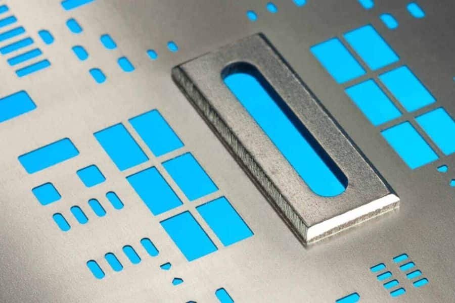
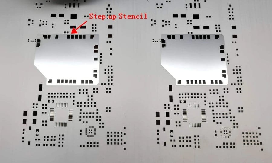
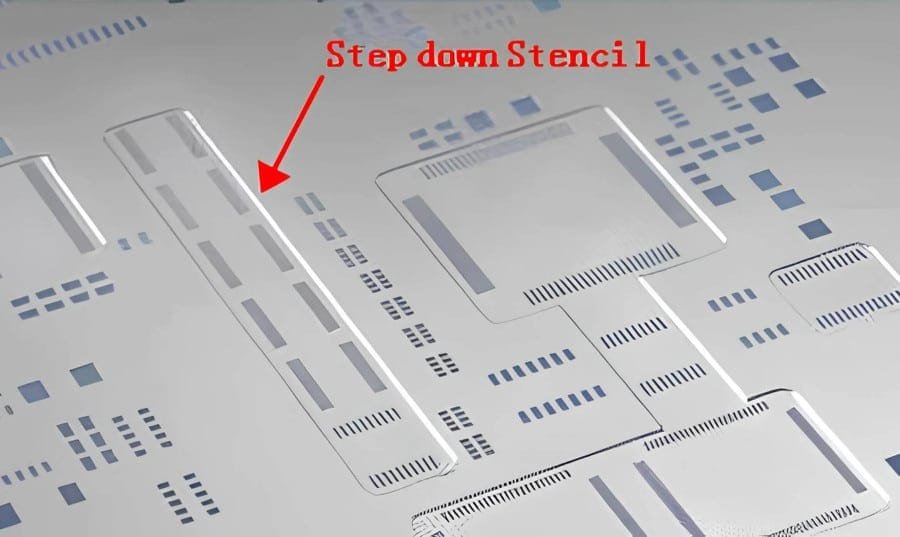
Step stencils are advanced tools used in PCB assembly to apply solder paste—a mixture of metal alloy and flux that forms electrical connections—onto PCBs, which are the backbone of electronic devices. Unlike standard stencils with uniform thickness, step stencils feature varying foil thicknesses to match the needs of different components. According to IPC 7525B Stencil Design Guidelines (2011), a step stencil is “a stencil with more than one foil thickness level.” This flexibility serves two key purposes:
- Step-Down Stencils: Thinner areas for small components (e.g., 01005 or 03015 metric parts) ensure proper area ratios for clean paste release, reducing defects in compact devices like smartphones.
- Step-Up Stencils: Thicker areas for larger components (e.g., BGAs, D-PAKs, or automotive edge connectors) deposit more paste, ensuring robust connections in high-power applications.
By customizing thickness, step stencils deliver consistent solder joints across diverse components, boosting reliability in everything from wearables to electric vehicle systems.
How Are Step Stencils Made?
Three primary methods are used in the U.S. to manufacture step stencils, each balancing precision, cost, and scalability:
- Photo-Chemical Etching:
- Process: A photographic resist protects areas of the foil, while etchant sprays remove material to create steps.
- Pros: Cost-effective for large-scale production; widely available.
- Cons: Less precise, often producing deeper step-downs than intended (e.g., 2.36 mils for a 2.0-mil target), which can affect paste volume control.
- Laser Welded Technology:
- Process: A section of the stencil is replaced with a foil of the desired thickness, laser-welded, and apertures are laser-cut.
- Pros: High precision, with step depths close to target (e.g., 2.08 mils for a 2.0-mil target); suitable for complex designs.
- Cons: Higher cost and longer production time due to welding complexity.
- Micro-Machining Technology:
- Process: A CNC milling machine removes material from a foil on a cooled vacuum plate, followed by laser-cutting apertures.
- Pros: Excellent accuracy (e.g., 2.01 mils for a 2.0-mil target); smooth surface finish enhances paste release.
- Cons: Equipment costs and slower processing for large volumes may limit scalability.
Experimental data shows laser welding and micro-machining achieve tighter standard deviations (0.15–0.19 mils) than etching (0.11–0.19 mils), making them ideal for high-precision applications like medical devices.
Experimental Insights: Testing Step Stencil Performance
Smith and Lentz conducted a printing experiment with 4-mil (101.6-micron) base stencils and step-down pockets of 2.0, 2.5, and 3.0 mils. Apertures targeted components like 03015 metric, 01005, 0.3 mm and 0.4 mm BGAs, and 0.5 mm pitch QFNs, placed 10, 20, 30, 40, and 50 mils from step edges. The study compared stencils with and without Fluoro-Polymer Nano (FPN) coating, using SAC305 Type 4 solder paste on bare copper boards.
Key Findings:
- Solder Paste Volume by Distance:
- Larger apertures (9.8 x 35.4 mils, for QFN leads) showed higher paste volumes at 10–20 mils from step edges compared to 30–50 mils, across all methods.
- Smaller apertures (e.g., 8 x 9 mils) had consistent volumes regardless of distance, ideal for fine-pitch components in compact devices.
- FPN Coating Benefits:
- FPN-coated stencils delivered higher paste volumes and lower variability, improving paste release and reducing defects.
- Method Accuracy:
- Etching overshot step depths (e.g., 1.69 mils for a 1.5-mil target), while welding and micro-machining were closer to nominal values, enhancing control.
These results suggest that FPN-coated, laser-welded, or micro-machined stencils are best for precision-critical applications, such as automotive control units or medical imaging systems.
Why Step Stencils Matter
Step stencils tackle the challenge of mixed-component PCBs, where tiny chips and large connectors coexist. They:
Ensure reliable solder joints, reducing failures in high-stakes applications like pacemakers or EV battery systems.
Minimize defects like insufficient or excess paste, cutting rework costs.
Streamline production by enabling a single stencil to handle diverse components, saving time in fast-paced industries like consumer electronics.
What’s Next for Step Stencil Technology?
Ongoing research aims to refine step stencils further, exploring:
- Paste volume differences between step centers and edges.
- Comparisons with non-stepped stencils of equivalent thickness.
- Effects of aperture orientation (horizontal vs. vertical) relative to squeegee motion.
- Impacts of varying squeegee pressure and speed on print quality.
These studies could unlock even greater precision, potentially reducing costs and expanding step stencil use in emerging fields like flexible electronics.
Conclusion
Step stencil technology is a cornerstone of modern PCB assembly, enabling manufacturers to meet the demands of increasingly complex and miniaturized electronics. From chemical etching’s affordability to laser welding’s precision and micro-machining’s smooth finishes, each method offers unique advantages. Experimental data confirms that FPN coatings and advanced manufacturing techniques deliver superior paste deposition, paving the way for reliable, high-quality PCBs in industries from smartphones to self-driving cars.
For your step stencil needs, contact JHYPCB, your trusted partner for precision stencil manufacturing. We specialize in laser-cut SMT stencils, step stencils, and nano-coating stencils to optimize your PCB assembly process. Reach out to our team at sales@pcbjhy.com to get started.
Related Reading
- The Main PCB Assembly Process Steps
- The Production Process and Specifications of PCB SMT stencil
- How to clean the solder paste on SMT stencil?
- 30 Common SMT PCB Assembly Defects
- Materials Used in Surface Mount Technology
- SMT PCB Assembly Manufacturing Process Introduces
- The Two Typical SMT Reflow Soldering Temperature Curve Modes
- Electronic PCB Assembly Process and Flow Chart
- Leveraging Turnkey PCB Assembly Manufacturing Services
- 3 Special Reminders for Printed Circuit Board Assembly (PCBA)
- What is Lead-Free Solder Paste (Pb-Free) in PCB Assembly?
- SPI in SMT Assembly: Enhancing PCB Quality Through Solder Paste Inspection
- Top 10 Factors to Consider When Choosing a PCB Assembly Company