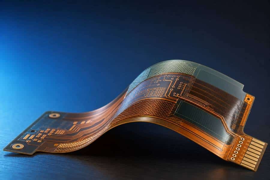
PCB Fabrication Quality Control
PCB Testing and Inspection for Bare Board Fabrication
At PCBELEC, PCB testing and inspection are integrated into our bare board fabrication workflow to help verify electrical integrity, structural consistency, and shipment quality before boards leave the factory.
From prototype builds to production orders, we apply appropriate testing methods based on board type, layer structure, impedance requirements, and end-use reliability expectations.
Need PCB assembly testing? Visit PCBJHY for PCBA services.
Why Bare PCB Testing Matters
A bare PCB may look acceptable on the surface while still containing internal or electrical defects that can affect assembly yield, signal integrity, insulation performance, or long-term reliability.
That is why PCB testing is not just a final checkpoint. It is an important part of verifying opens and shorts, plated hole quality, impedance consistency, dimensional accuracy, and the structural condition of the finished board before shipment.
- Detect opens and shorts
- Verify plated hole integrity
- Confirm impedance consistency
- Reduce downstream assembly risk
Learn more about our PCB fabrication process and Quality & Engineering Support.
Our Bare PCB Testing and Inspection Capabilities
We select testing and inspection methods according to the board structure, project stage, and customer specification, with a focus on bare board fabrication quality rather than post-assembly functional testing.
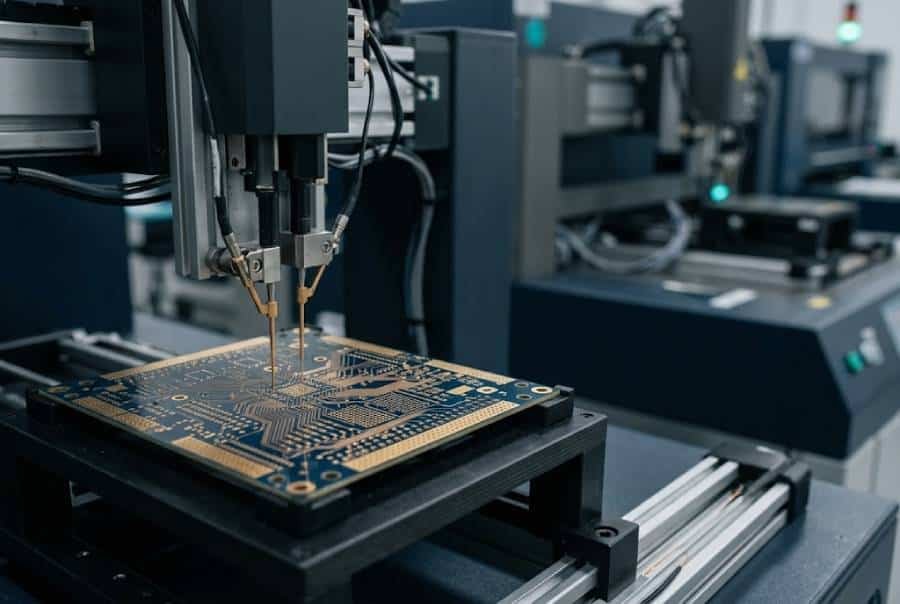
Bare Board Electrical Testing
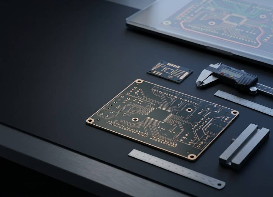
Bare board electrical testing is one of the most essential verification steps in PCB fabrication. It is used to confirm circuit continuity and detect open circuits or short circuits before the boards move to shipment or downstream assembly.
Best for: Standard rigid and multilayer PCB orders.
Related page: PCB manufacturing capabilities
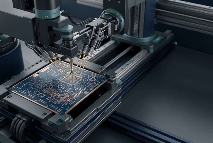
Flying Probe Testing
Flying probe testing is a practical option for prototype PCB, engineering samples, and low-volume fabrication runs because it can verify electrical connections without the cost and lead time of dedicated fixtures.
Best for: Prototype and high-mix, low-volume projects.
Related page: Prototype PCB services
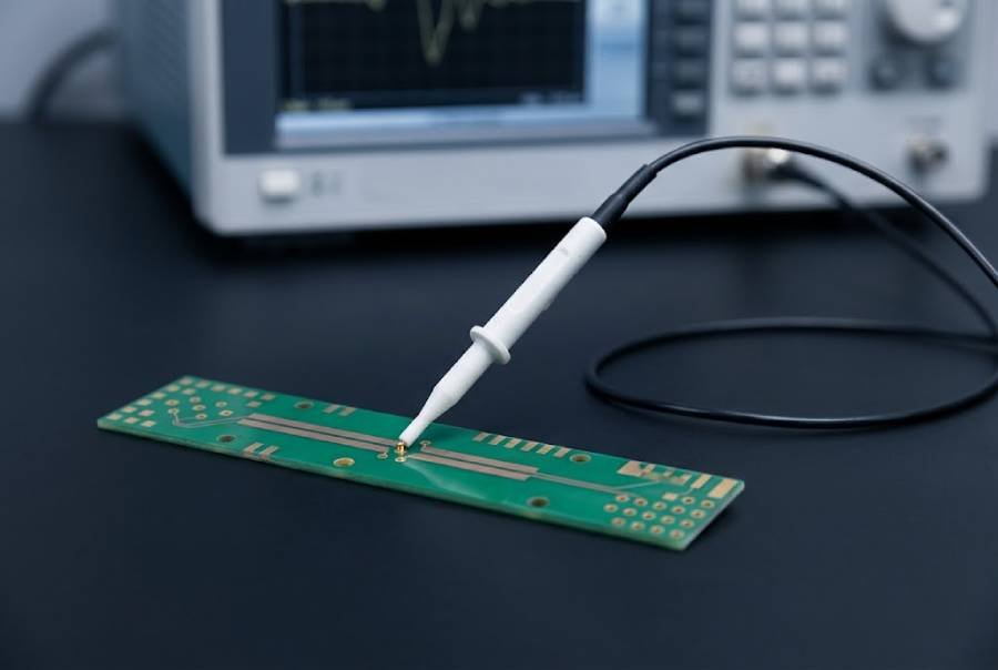
TDR Impedance Testing
TDR testing is used to verify controlled impedance performance on boards designed for high-speed signal transmission or RF applications. It helps confirm that finished structures remain within the specified impedance range.
Best for: High-speed and impedance-control PCB projects.
Related pages: High Frequency PCB | Impedance Control PCB
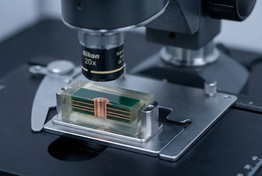
Microsection Analysis
Microsection analysis helps evaluate plated through holes, copper thickness, lamination structure, interface bonding, and layer alignment through cross-sectional inspection of the finished board.
Best for: Multilayer, HDI, and reliability-sensitive PCB projects.
Related pages: Multilayer PCB | HDI PCB
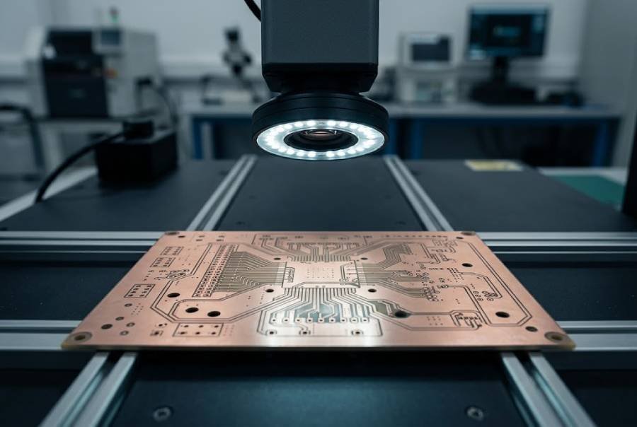
Visual Inspection and AOI for Bare Boards
Visual inspection and AOI can help identify bare-board manufacturing issues such as pattern defects, etching irregularities, registration deviation, contamination, and other visible nonconformities before shipment.
Best for: Routine fabrication quality checks.
Related page: Quality & Engineering Support
Dimensional and Reliability Verification
Depending on board type and application, additional checks may include dimensional measurement, insulation testing, dielectric withstand verification, thermal stress testing, and selected environmental reliability validation.
Best for: Industrial, high-temperature, or demanding-use boards.
Related pages: High Tg PCB | Heavy Copper PCB
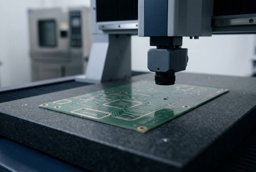
Testing Methods at a Glance
The table below provides a quick overview of what each testing method checks and where it is most commonly applied in bare PCB fabrication.
| Test / Inspection | What It Checks | Typical Use Case |
|---|---|---|
| Bare Board Electrical Test | Detects open circuits and short circuits by verifying basic electrical continuity. | Standard rigid PCB and multilayer PCB fabrication orders before shipment. |
| Flying Probe Test | Verifies net connectivity without dedicated fixtures and supports flexible test programming. | Prototype PCB, engineering samples, and low-volume fabrication projects. |
| TDR Impedance Test | Measures controlled impedance performance for high-speed or signal-sensitive structures. | High frequency PCB and impedance-control PCB projects. |
| Microsection Analysis | Checks plated hole quality, copper thickness, lamination structure, and internal bonding conditions. | Multilayer PCB, HDI PCB, and reliability-sensitive applications. |
| Visual Inspection / AOI | Identifies visible manufacturing defects such as pattern irregularities, registration deviation, contamination, and surface nonconformities. | Routine bare board fabrication quality checks. |
| Dimensional & Reliability Validation | Confirms dimensional accuracy, insulation performance, dielectric withstand capability, and selected reliability requirements. | Industrial, high-temperature, high-voltage, or harsh-environment PCB projects. |
Testing Methods by PCB Type and Project Need
Different PCB structures call for different verification priorities. The following examples show how testing focus may change by board type and project requirement.
Prototype PCB
Prototype projects often need fast-turn verification to confirm electrical integrity and uncover fabrication issues early, before a design moves into larger production quantities.
High Frequency and Impedance-Control PCB
Boards designed for controlled impedance and fast signal transmission require closer attention to transmission-line consistency, material behavior, and fabrication accuracy.
Multilayer and HDI PCB
As layer count and board density increase, internal quality becomes more critical. These projects often benefit from microsection analysis, plated hole evaluation, and tighter structural verification.
High-Reliability PCB Projects
Boards used in demanding environments may require broader validation beyond standard fabrication checks, including insulation resistance, thermal stress, and selected environmental testing.
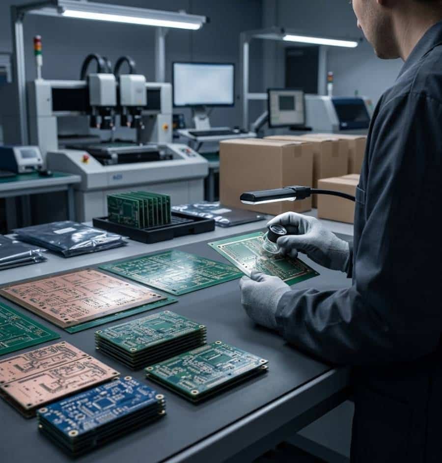
How We Verify PCB Quality Before Shipment
1. Gerber and CAM Review
Before fabrication begins, design data is reviewed for manufacturability and process compatibility so potential production risks can be identified earlier.
2. In-Process Fabrication Inspection
During production, key fabrication stages are monitored to help identify visible or structural issues before the board reaches final release.
3. Electrical Verification
Finished bare boards undergo electrical checking to verify continuity and detect open or short conditions according to project requirements.
4. Advanced Validation When Required
For projects with tighter specifications, additional testing may include impedance measurement, microsection analysis, dimensional verification, insulation testing, or selected reliability validation.
5. Final Inspection and Shipment Release
Boards are released for shipment only after required inspection and testing steps are completed according to the order’s fabrication and quality requirements.
Learn more about our broader quality management process.
Additional Reliability and Validation Options
For projects with more demanding technical or environmental requirements, additional validation can be applied to support product quality expectations.
- Ion contamination testing
- Adhesion / peel testing
- Thermal stress testing
- Moisture and insulation resistance testing
- Cold and thermal shock testing
- Solvent resistance testing
- Dielectric withstand validation
- Special-environment testing on request
Quality Standards and Engineering Support
Testing and inspection requirements can be matched to customer documentation, product specifications, and applicable PCB quality standards.
These inspections are part of a broader quality workflow that also includes engineering review, process control, and shipment release management.
- IPC-6012
- IPC-6013
- IPC-6016
- IPC-6018
- Customer specifications
- Project-based verification
See our Quality & Engineering Support page for the full quality workflow.
Need PCB Assembly Testing Instead?
PCBELEC focuses on bare PCB fabrication only. For SMT, THT, BGA inspection, ICT, FCT, turnkey PCBA, and other assembly-stage testing needs, please visit PCBJHY for dedicated support.
Need a PCB Fabrication Quote?
Send your Gerber files, layer count, material requirements, thickness, copper weight, impedance targets, and testing needs for a custom quotation and engineering review.
We support prototype-to-production bare PCB fabrication projects.