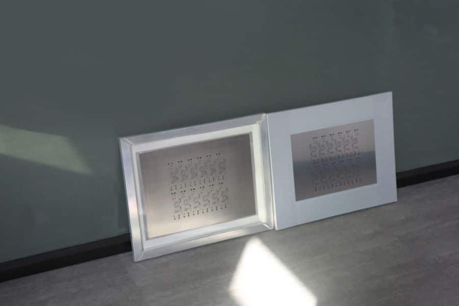
Custom Electroform Stencils for SMT Assembly

What is an Electroform Stencil?
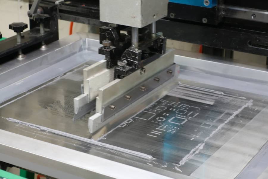
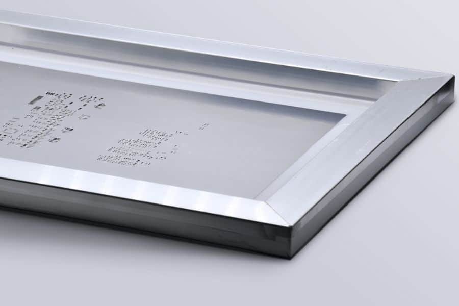
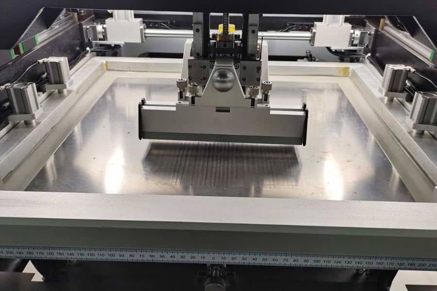
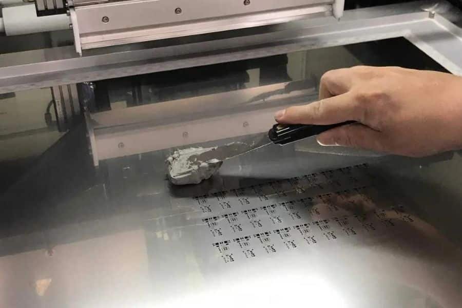
An electroform stencil is a high-precision SMT stencil custom-manufactured through an electroforming process. Featuring ultra-smooth, trapezoidal aperture walls, these stencils are designed to meet client-specific requirements for fine-pitch and ultra-fine-pitch components, delivering exceptional solder paste release and transfer efficiency of 95% or higher.
Key Features of Custom Electroform Stencils
- Tailored Paste Release: Smooth trapezoidal sidewalls, customized for your design, outperform polished laser or etched stencils, ensuring 95%+ paste transfer efficiency and minimal bridging.
- Ultra-Precise Apertures: Aperture tolerances within +/- 10 microns (.0004”), engineered for fine-pitch components as small as 0.3mm.
- Enhanced Durability: Nickel electroform foils (hardness 500 Hv or higher) are harder than stainless steel, providing longer stencil life for high-volume client projects.
- Low Friction: Nickel’s lower friction coefficient improves paste rolling and reduces squeegee blade wear, optimized for your SMT process.
- Fully Customizable: Framed or frameless designs, with thicknesses from 1 to 12 mils in 0.1 mil increments, including non-standard thicknesses and step/relief areas (e.g., 2.4, 4.2, 5.7 mils) to match your specifications.
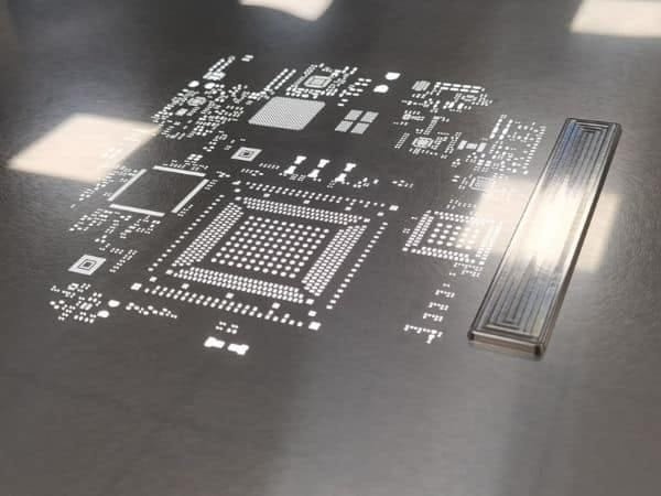
- High Aperture Count Efficiency: Supports dense, client-designed image areas with unlimited pad counts, free from heat distortion caused by laser cutting.
- Optimized for Yield: Custom thinner stencils improve paste transfer, reducing defects and boosting process yields for your production.
- Rapid Customization: Fast production for large aperture counts, tailored to your project timelines.
Nickel has a lower coefficient of friction compared to stainless steel
Applications
JHYPCB’s custom electroform stencils are ideal for industries requiring precision and reliability, including.


How Electroforming Works
Our electroforming process ensures precision tailored to your design specifications:
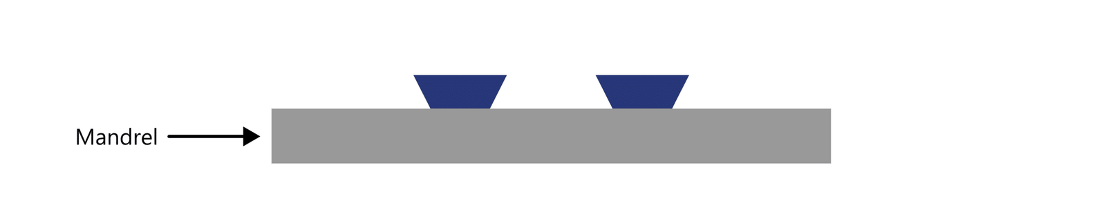
Step 1
Step 1
A resist layer on a mandrel is imaged using a client-provided master photoplot.
Step 2
Step 2
Undeveloped resist is stripped, leaving pillars of developed resist.
Step 3
Step 3
The mandrel is immersed in a nickel bath, where nickel atoms are deposited following the electrical current.
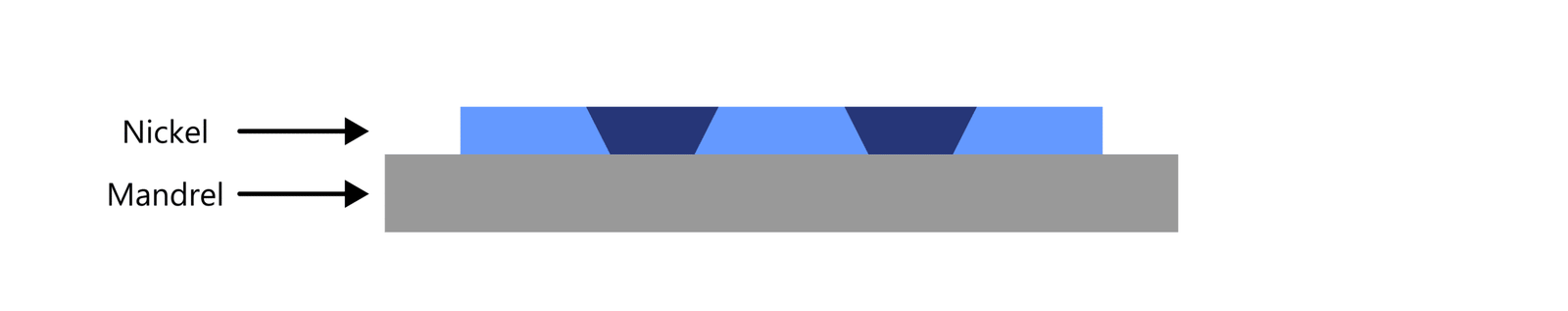
Step 4
Step 4
After removal from the mandrel and stripping of remaining resist, a custom nickel stencil is produced to exact specifications.


Why Choose JHYPCB for Custom Electroform Stencils?
At JHYPCB, we specialize in custom manufacturing, delivering electroform stencils designed to your exact specifications, just like our step stencil, Nano-coating stencil, PCB manufacturing, and assembly services. We ensure high precision, durability, and efficiency using advanced electroforming technology and stringent quality control. With options for framed or frameless designs, customizable thicknesses, and rapid turnaround, our stencils are crafted to enhance your SMT assembly process, reduce defects, and maximize yields.
Available Sizes
| Thickness(mil) | Max foil size | Thickness Tolerance | Min aperture size | Min gap b/w openings |
|---|---|---|---|---|
| 0.5 to 1.0 | 12″ x 12″ | +/-0.0001″ | 0.002″ | 0.003″ |
| 1.0 to 2.0 | 18″ x 18″ | +/-0.0002″ | 0.003″ | 0.004″ |
| 2.0 to 3.0 | 21.5″ x21.5 | +/-0.0003″ | 0.004″ | 0.004″ |
| 3.0 to 4.0 | 21.5″ x24 | +/-0.0004″ | 0.0045″ | 0.005″ |
| 4.0 to 5.0 | 21.5″ x 24″ | +/-0.0004″ | 0.005″ | 0.006″ |
| 5.0 to 6.0 | 21.5″ x 24″ | +/-0.0005″ | 0.006″ | 0.006″ |
| 6.0 to 7.0 | 21.5″ x 24″ | +/-0.0005″ | 0.0075″ | 0.0075″ |
| 7.0 to 8.0 | 21.5″ x 24″ | +/-0.0005″ | 0.0075″ | 0.0075″ |