






Quick Turn PCB Assembly: A Timeline Planning Guide for Faster Delivery
What actually determines your PCB assembly lead time — and how to prepare files, BOM, and design choices to get the fastest possible turnaround without quality surprises.
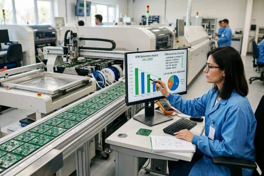
Quick turn PCB assembly isn’t just about a supplier promising “fast delivery.” Real speed comes from preparation: complete documentation, available components, DFM-ready designs, and understanding which factors add days to your timeline. This guide breaks down the 5 stages of assembly lead time and shows you how to shrink each one.
For expedited assembly — including 24–48 hour turnaround on in-stock components — our partner brand JHYPCB operates dedicated quick-turn assembly lines from its Shenzhen facility.
Explore assembly capabilities · Get an expedited quote · Upload your BOM
The 5 Stages of PCB Assembly Lead Time
Most teams underestimate how many stages exist between sending files and receiving assembled boards. Each stage has its own time cost — and its own opportunities to save time if you prepare well.
Stage 1: Quotation and DFM Review (0.5–2 days)
The clock starts when the supplier receives your files. If your BOM is incomplete, Gerber files have issues, or component availability is unclear, the quote stalls while the supplier emails you back and forth.
How to shrink it:Send complete documentation on day one —
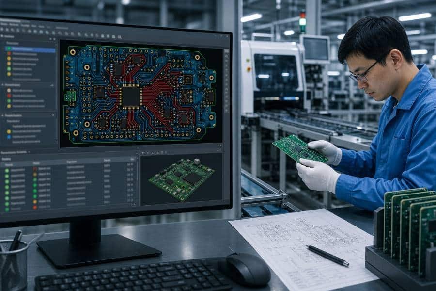
Gerber (RS-274X or ODB++), full BOM with manufacturer part numbers and approved equivalents, pick-and-place file, and any assembly drawings. A DFM-ready package lets the supplier start immediately.
Stage 2: Component Sourcing (1–7 days)
This is the most unpredictable stage. If you chose turnkey sourcing, the supplier must purchase all components. Standard parts (0603/0805 resistors, common ICs) are usually in stock. But specialized parts — BGAs, scarce ICs, long-lead microcontrollers — can add days or weeks.
How to shrink it:
Use commonly available components and always list 2–3 approved alternatives in your BOM. Avoid sole-source parts unless absolutely necessary. If you have hard-to-find components in stock locally, consider consigned (kitted) assembly to eliminate sourcing wait entirely.
Stage 3: PCB Fabrication (2–5 days)
If your supplier also fabricates the bare board (as PCBELEC does), fabrication runs in parallel with component sourcing. Simple 2–4 layer boards can be done in 24–48 hours. Complex HDI or high-layer count boards take longer.
How to shrink it:
Keep the design simple for prototype builds — standard FR-4, standard via sizes, no blind/buried vias unless required. PCBELEC offers 24-hour fabrication for simple prototypes.
Stage 4: Assembly Production (1–3 days)
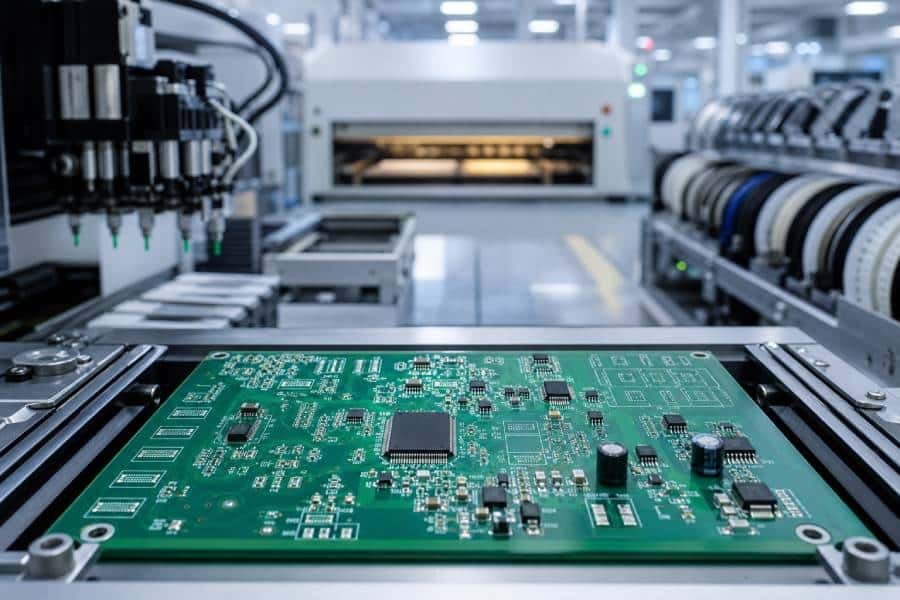
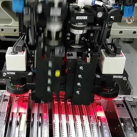
Once boards and components arrive, SMT placement and soldering typically takes 1–2 days for prototype quantities. THT (through-hole) components add manual labor time. BGA parts require X-ray verification.
How to shrink it: Minimize THT components in your prototype. If you use BGAs, confirm the supplier has X-ray capability in-house (rework without X-ray is risky). Panelize efficiently — a
well-designed panel lets the pick-and-place machine run without interruption.
Stage 5: Testing and Shipping (1–2 days)
AOI inspection is fast (minutes). X-ray adds slightly more time. ICT/FCT requires custom test fixtures — for prototypes, consider deferring full functional testing to a later build stage. Shipping via express courier (DHL/FedEx) takes 2–5 days to most destinations.
How to shrink it: For prototypes, request AOI only (standard at JHYPCB). Reserve ICT/FCT for production verification builds. Choose express shipping with tracking.
Design Choices That Speed Up (or Slow Down) Assembly
Your design decisions directly impact how fast a supplier can assemble your boards. These are the most common speed bottlenecks:
| Design Choice | Fast | Slow |
|---|---|---|
| Component packages | 0603, 0805, standard ICs | 0201, 01005, custom packages |
| BGA usage | No BGA, or standard pitch (≥0.8mm) | Fine-pitch BGA (≤0.5mm), requires X-ray |
| Via types | Through-hole only | Blind/buried microvias (longer fab time) |
| Component sourcing | Standard parts, 2–3 alternatives listed | Sole-source, obsolete, or allocation-affected parts |
| Panelization | Single design, V-score or tab-routing | Mixed designs on one panel (more setup time) |
| Surface finish | HASL (fastest, cheapest) | ENIG (needed for BGA, adds 0.5–1 day) |
| Testing | AOI only | AOI + X-ray + FCT (fixture required) |
| THT components | None or minimal | Many THT parts (manual soldering) |
Rule of thumb: If speed is your #1 priority for a prototype, simplify aggressively. Save the advanced features for the production design where lead time is less critical.

Quick Turn Assembly Checklist — What to Prepare
Before sending files to any quick-turn assembly partner, make sure you have:
Files:
✅ Gerber files (RS-274X or ODB++) — latest revision only
✅ BOM with manufacturer part numbers, quantities, and 2–3 approved alternatives per critical component
✅ Pick-and-place file (CPL/XY data) with correct rotation and coordinates
✅ Assembly drawings (if hand placement or special instructions needed)
Design
✅ DFM check completed (no unmanufacturable features)
✅ Component footprints verified against actual parts
✅ Panelization design ready (if ordering multiple boards)
✅ Test points accessible (if ICT/FCT is planned)
Logistics
✅ Target lead time defined and communicated
✅ Shipping address and customs requirements confirmed
✅ Incoterm agreed (DAP, DDP, or EXW)
✅ Accepted alternatives for scarce components pre-approved
Having all of this ready can save 2–3 days compared to a typical back-and-forth quoting process. JHYPCB typically provides quotes within 24 hours for complete submission packages.
FAQs
For simple 2–4 layer boards with in-stock components, JHYPCB offers 24–48 hour assembly after files and components are confirmed. More complex builds — high layer count, BGA, turnkey sourcing — typically take 3–7 working days. The biggest variable is component availability, not the assembly process itself.
Quick turn assembly prioritizes speed through expedited scheduling, dedicated lines, and minimized setup time. Standard assembly follows normal production queue sequencing. Quick turn typically costs 20–50% more but can cut lead time by 50–70%. For prototypes where time-to-market is critical, the premium is usually justified.
No. JHYPCB's quick turn service still includes AOI (Automated Optical Inspection) as standard. X-ray inspection for BGA joints is also available on quick turn builds. What's typically reduced is not inspection, but queue wait time and setup time — the actual assembly and testing process follows the same quality standards.
Yes. PCBELEC manufactures bare boards (24–48 hours for simple prototypes) and JHYPCB assembles them — both from the same Shenzhen facility. Running fabrication and component sourcing in parallel can compress total timeline to 5–7 days for a complete prototype build, compared to 10–14 days with sequential vendors.
The #1 delay cause is incomplete or inaccurate BOM data — missing manufacturer part numbers, no approved alternatives, or obsolete components. The #2 cause is DFM issues discovered after production starts (wrong footprints, unmanufacturable features). Both are preventable with proper preparation before submitting files.
Send Gerber files (RS-274X or ODB++), a complete BOM with manufacturer part numbers and 2–3 approved equivalents, pick-and-place data (CPL/XY), and any assembly drawings — all in one package. Clearly state your target lead time and quantity. Complete packages can receive quotes within 24 hours from JHYPCB.
Ready to Start Your Quick Turn Project?
Send your BOM, Gerber files, and target lead time to JHYPCB for an expedited quote — typically returned within 24 hours.
Need bare boards fabricated first?
PCBELEC offers 24-hour prototype PCB fabrication.
Contact us at sales@pcbelec.com.