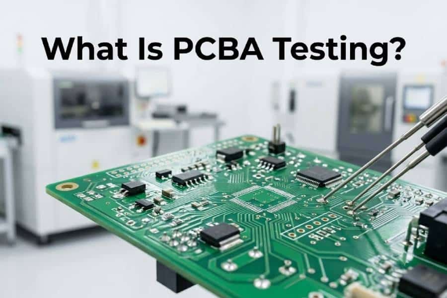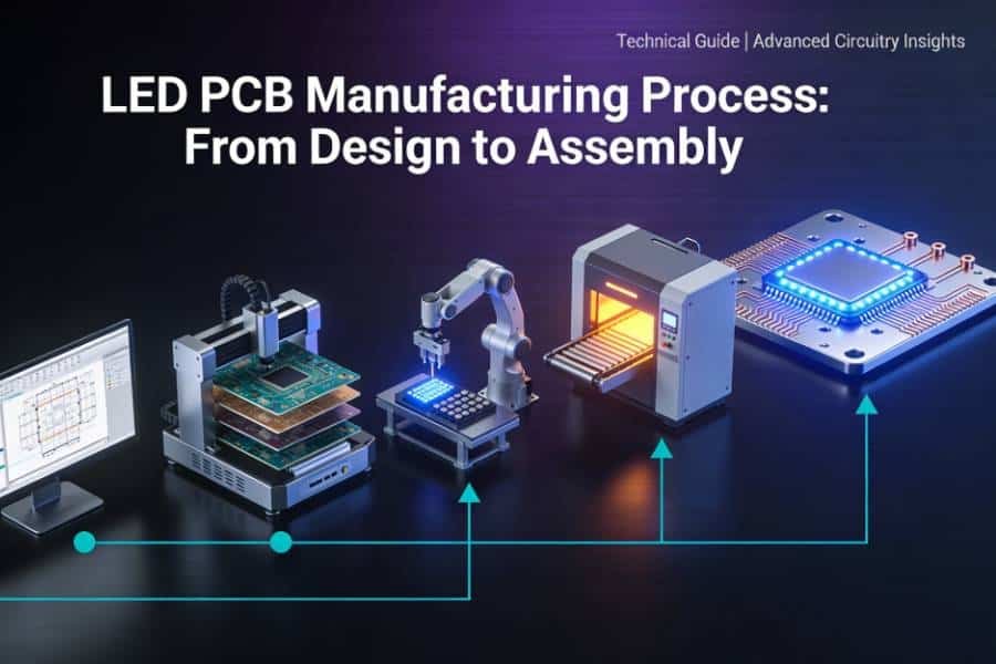
Table of Contents
In the ever-expanding world of electronics, where applications span from sleek consumer gadgets to rugged industrial systems and high-stakes aerospace tech, the Printed Circuit Board (PCB) stands as the unsung hero holding it all together. At JHYPCB, with over a decade of experience as a leading China-based PCB manufacturer specializing in everything from prototypes to multi-layer rigid, flexible, and rigid-flex PCBs, we’ve seen firsthand how soldering quality can make or break a device’s performance. Soldering defects are a common culprit behind electronic failures, often stemming from improper techniques or overlooked parameters during assembly.
Whether you’re prototyping a new design, handling repairs, or scaling up production, mastering how to solder on PCB is crucial for creating sturdy, durable joints that withstand operational stresses like vibration, heat, and humidity. In this in-depth article, we’ll dive deeper than the basics, covering various soldering techniques, key considerations for Surface Mount Technology (SMT) components, rework strategies, and real-world tips drawn from our expertise in PCB manufacturing and assembly services—including SMT, Through-Hole Technology (THT), mixed tech, turnkey assembly, and component sourcing. We’ll also weave in insights from our related resources to help you build a stronger knowledge base.
What is PCB Soldering? A Foundation for Reliability
At its core, PCB soldering is the process of metallurgically joining electronic components to the PCB using a molten solder alloy that solidifies into a strong mechanical and electrical connection. This step is pivotal in PCB assembly, transforming a bare board into a functional circuit.
Gone are the days of leaded solders dominating the scene; today, lead-free soldering reigns supreme, driven by global environmental regulations like RoHS. Lead-free options, such as SAC (Tin-Silver-Copper) alloys, offer excellent reliability while minimizing ecological impact. But choosing the right solder isn’t just about compliance—it’s about matching melting points, flow characteristics, and compatibility with your components to avoid issues like brittle joints or intermetallic growth.
For those curious about lead-free specifics, check out our detailed post on What is Lead-Free Solder Paste (Pb-Free) in PCB Assembly?, where we break down formulations, benefits, and selection tips tailored for modern assemblies.
Exploring the Key Soldering Techniques in PCB Assembly
Soldering methods have evolved alongside PCB complexity, balancing factors like precision, cost, volume, and component types. Here’s a closer look at the primary techniques on how to solder on PCB, with pros, cons, and when to use each—enhanced with our practical insights from handling thousands of projects.
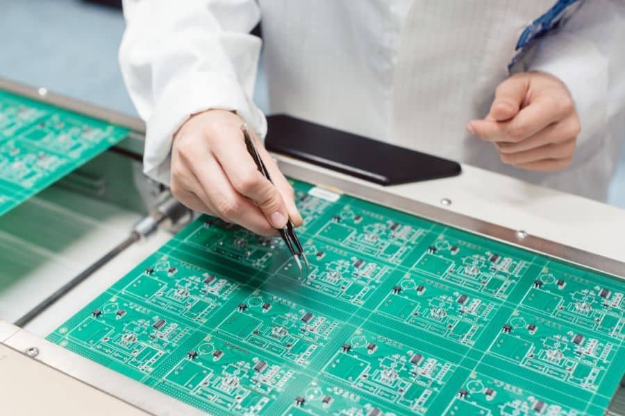
1. Hand Soldering: The Versatile Manual Approach
Hand soldering remains a go-to for low-volume work, prototypes, repairs, or attaching through-hole components. Using a soldering iron (typically 25-60W for precision), you melt solder wire onto pads and leads, forming joints manually.
- Steps for Success: Clean surfaces with flux to remove oxides, heat the joint evenly (not the iron tip directly), and apply solder for a shiny, concave fillet. Avoid overheating to prevent lifted pads or cold joints.
- Pros: Low cost, flexible for rework; ideal for flex PCBs where delicacy is key.
- Cons: Labor-intensive, prone to human error in high volumes.
- Tip from JHYPCB: For flexible circuits, temperature control is vital to avoid delamination. Dive deeper in our guide How to Solder On Flex PCB? for specialized techniques.
This method shines in prototyping but scales poorly—transition to automated options for production.

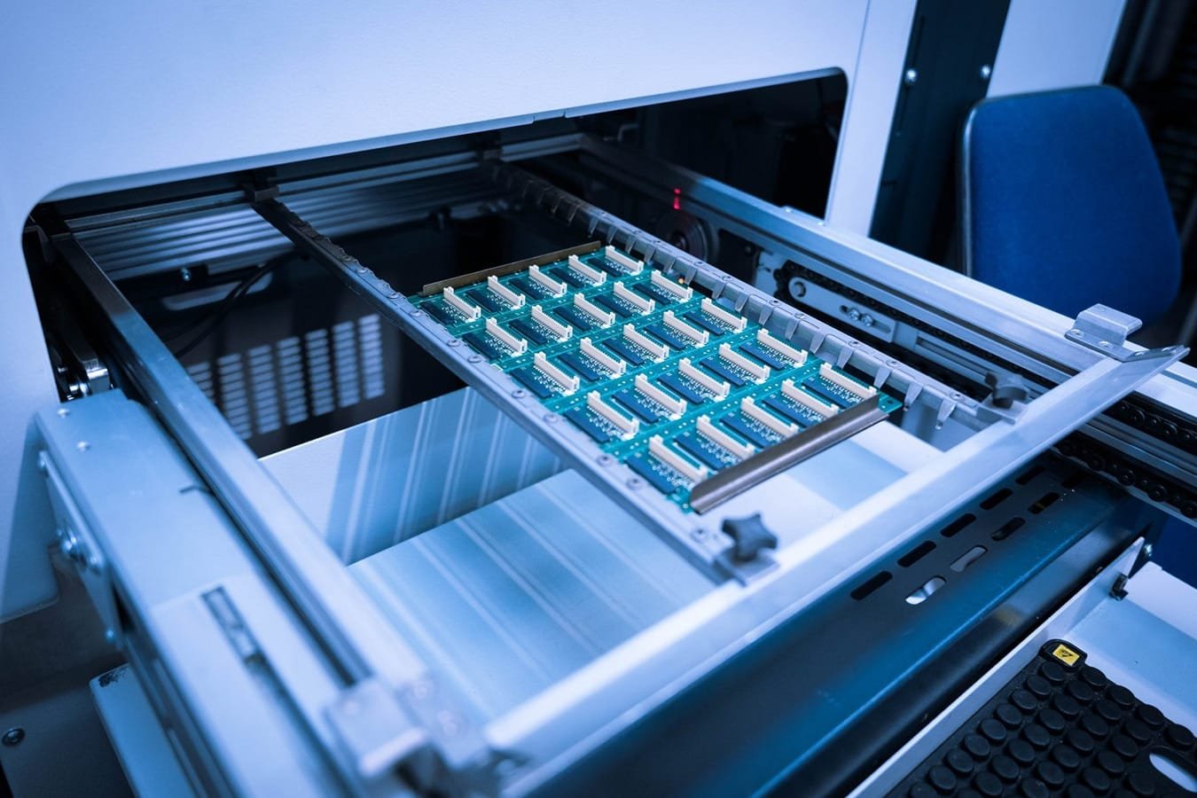
2. Wave Soldering: Efficient for Through-Hole Components
Wave soldering automates the process for through-hole parts by passing the PCB over a molten solder “wave” in a conveyor system.
- Key Steps:
- Flux Application: Coats leads to promote wetting and prevent oxidation.
- Pre-Heating: Gradually raises board temperature (around 100-150°C) to evade thermal shock.
- Solder Wave Contact: The board dips into the wave (typically 260°C for lead-free), soldering exposed leads.
- Cooling: Solidifies joints in a controlled chamber.
- Pros: High throughput, cost-effective for medium volumes.
- Cons: Not suited for dense SMT boards; risks solder bridging.
- JHYPCB Insight: We’ve optimized wave processes for mixed assemblies—see our Selective Wave Soldering Guidelines for handling hybrid PCBs without damaging sensitive parts.
Compare this to reflow in our comparison article Reflow Soldering VS. Wave Soldering: What’s the Difference? to decide what’s best for your design.

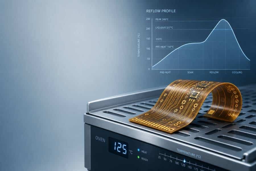
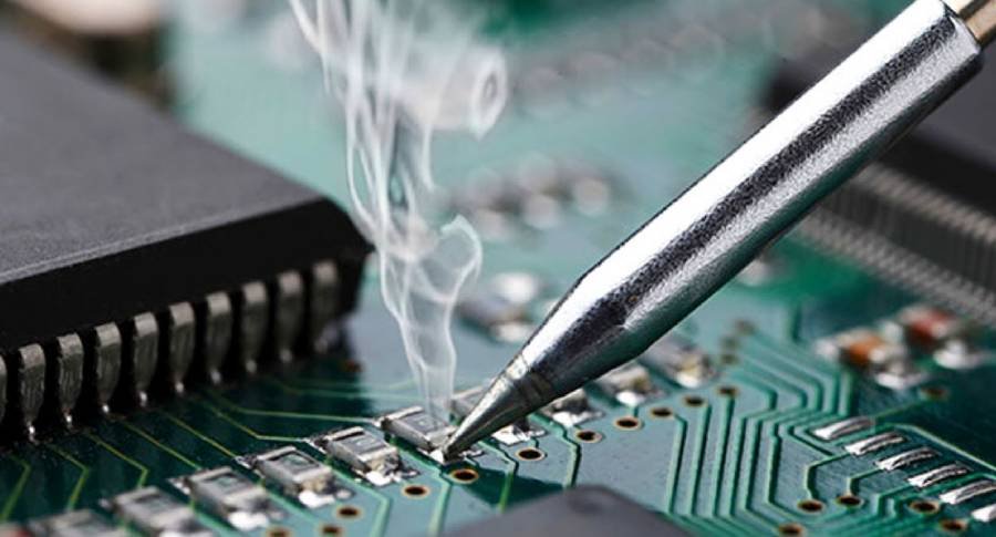
3. Reflow Soldering: The SMT Powerhouse
Reflow soldering dominates SMT assembly, where components sit on surface pads without holes, saving space and enabling miniaturization.
- Process Breakdown:
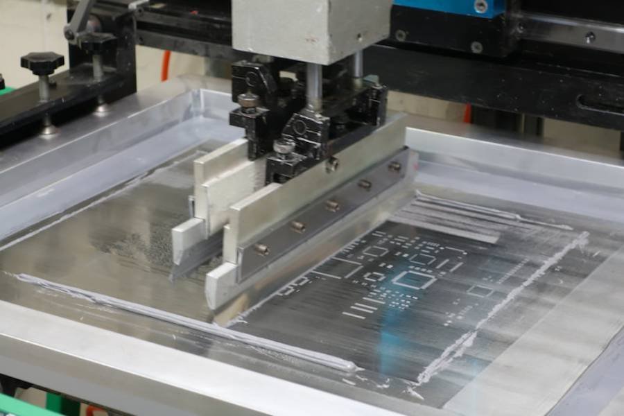
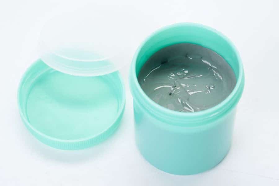
- Solder Paste Printing: Apply paste (a mix of solder particles and flux) via stencil onto pads. For stencil tips, read How to Clean the Solder Paste on SMT Stencil? to maintain precision.
- Component Placement: Pick-and-place machines mount parts on wet paste.
- Reflow Oven: Boards pass through zones following a thermal profile—preheat, soak, reflow (peak ~245-260°C), and cool—to melt and cure solder.
- Pros: Precise, scalable for high-density boards; self-aligns components.
- Cons: Requires accurate profiles to avoid tombstoning or voids.
- Expert Tip: Optimize curves for reliability—explore Optimized SMT Reflow Soldering Temperature Curves: Warm-Up vs. Gradual Heating for reducing defects.
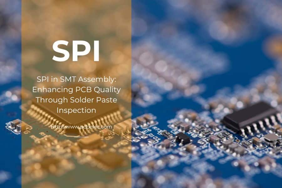
Don’t forget quality checks; our post on SPI in SMT Assembly: Enhancing PCB Quality Through Solder Paste Inspection details how 3D inspection catches paste issues early.
For paste fundamentals, refer to Solder Paste and Solder Paste Printing in SMT PCB Assembly.

4. Selective Soldering: Precision for Mixed Assemblies
When your PCB mixes SMT and through-hole, selective soldering targets specific areas with a programmable nozzle or mini-wave, sparing nearby components.
- Advantages: Reduces masking needs, minimizes thermal stress.
- Applications: Ideal for connectors or large capacitors in dense designs.
- Consideration: Programming accuracy is key for repeatability.
This technique bridges gaps in hybrid boards, enhancing overall efficiency.

Critical Considerations for Soldering SMT Components
SMT demands attention to detail for flawless results. Here’s what to prioritize:
- Solder Pad Design: Opt for Non-Solder Mask Defined (NSMD) pads for better control and alignment—larger than footprints to allow self-centering.
- Solder Paste Selection: Factor in particle size (Type 3-5 for fine-pitch), alloy (e.g., low-voiding for BGAs), and no-clean vs. water-soluble flux. Compatibility with stencils ensures even deposition.
- Thermal Profiling: Follow datasheet ramps (1-3°C/sec) to prevent warpage. Peak too high? Risk component damage; too low? Weak joints.
- Stencil Optimization: Thickness (100-150µm) and aperture ratios (0.6-1.0) dictate paste volume—laser-cut with electropolish for release.
These elements tie into broader assembly quality, reducing rework and boosting yield.
Mastering PCB Soldering During Rework: Step-by-Step Guide
Even the best processes need fixes. Rework corrects defects like misalignments or failed joints, following IPC standards for safety.
- Preheat the Board: Bake at 80-100°C to drive out moisture and ease desoldering.
- Heat to Liquidus: Use hot air (300-350°C) to melt old solder without scorching.
- Clean Pads: Wick away residue with fluxed braid for a fresh surface.
- Apply New Paste: Stencil or dispense precisely to avoid excess.
- Reflow Selectively: Hot air or IR for targeted heating, sparing other parts.
- Inspect Thoroughly: Visual, X-ray, or AOI to spot voids or bridges.
Pro tip: Minimize reflow cycles to preserve board integrity—our experience shows selective tools cut risks by 50%.
Common Mistakes to Avoid and Pro Tips from JHYPCB
- Overheating: Leads to lifted pads—always monitor temps.
- Insufficient Flux: Causes poor wetting; use generously but clean residues.
- Ignoring Profiles: Skimping here invites defects—calibrate ovens regularly.
- Long-Tail Insight: For queries like “best practices for how to solder on PCB without defects,” integrate inspection early, as in SPI, for 99%+ yields.
At JHYPCB, we’ve refined these techniques through countless turnkey projects, ensuring your PCBs endure real-world demands.
Conclusion: Elevate Your PCB Soldering with Expert Support
Understanding how to solder on PCB isn’t just technical—it’s about crafting reliable, long-lasting electronics that perform under pressure. From hand soldering’s simplicity to reflow’s precision, each technique has its place, and blending them with SMT best practices yields superior results.
If you’re tackling a new project or need custom PCB manufacturing, assembly, or even SMT stencils, our team at JHYPCB is here to help. With services covering prototypes, multi-layer boards, flex/rigid-flex options, and full component sourcing, we deliver quality that meets global standards. Reach out to us at sales@pcbjhy.com for quotes, technical advice, or tailored solutions. Let’s build something exceptional together!