


Table of Contents
Introduction to PCB Assembly Welding
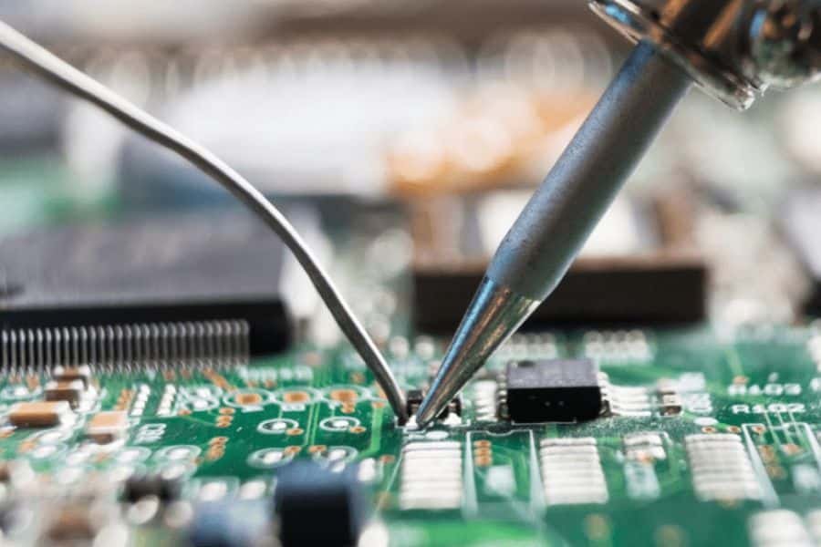
PCB assembly is a critical step in electronics manufacturing, where components are soldered onto a PCB to create functional circuits. The choice of PCB assembly welding process impacts production costs, efficiency, and product reliability. This article examines five key circuit board welding processes, enabling designers and manufacturers to optimize their PCB production for both cost and performance.
Whether you’re designing a single-sided PCB for a budget-friendly device or a complex multilayer board for advanced electronics, understanding these processes is key. Read on to discover how to select the right PCB assembly process for your project and reduce costs without compromising quality.

Key Considerations in PCB Design and Assembly
Before diving into the welding processes, consider these factors that influence your choice of PCB assembly process:
- PCB Type: Single-sided, double-sided, or multilayer PCBs affect the complexity and cost of soldering. Multilayer PCBs allow more circuits in less space but increase production costs.
- Component Type: Through-hole (PTH) components are durable but bulky, while Surface-Mount (SMT) components enable compact designs.
- Welding Approach: Single-sided welding is simpler and cheaper, but double-sided welding maximizes board space.
- Design for Manufacturability (DFM): Consult your SMT manufacturer early to align your design with their capabilities, especially for processes like red glue or selective wave soldering.
5 Essential PCB Assembly Welding Processes
1. Single-Sided Through-Hole Assembly (Wave Soldering)
Process: Components with through-hole (PTH) pins, such as resistors, capacitors, and inductors, are manually inserted into a single-sided PCB. The board then passes over a wave of molten solder in a wave soldering machine to secure the components.
Applications
This process is used in low-cost electronics like power supplies, transformers, and mouse boards, where PTH components handle high current or voltage.
Advantages
- Cost-effective: Requires only one soldering process.
- Simple setup: Ideal for basic designs with large components.
Disadvantages
- Larger board size: PTH components take up more space than SMD components.
- Declining use: Less common due to the popularity of SMT technology.
Cost Considerations
Wave soldering is economical for simple designs but less suited for compact, modern PCBs. Check with your EMS manufacturer for DFM guidelines to optimize component placement.

2. Single-Sided SMT + Wave Soldering
Process: Solder paste is printed on a single-sided PCB, followed by placement of Surface-Mount Devices (SMDs) and reflow soldering to secure them. Then, PTH components are inserted and soldered using wave soldering.
Applications
This process suits consumer electronics with a mix of SMD and PTH components, balancing cost and design complexity.
Advantages
- Cost-effective: Combines SMT for compact components with wave soldering for durable PTH parts.
- Smaller PCB size: SMDs reduce board footprint compared to full PTH assembly.
Disadvantages
- Two processes: Requires separate SMT and wave soldering lines, increasing setup costs.
- Limited flexibility: Not ideal for double-sided designs.
Cost Considerations
This SMD + DIP approach is popular for its balance of cost and performance. Avoid wave soldering if possible, as heating the furnace is energy-intensive.

3. Double-Sided SMT + Red Glue + Wave Soldering
Process: The first side undergoes solder paste printing, SMD placement, and reflow soldering. The second side uses red glue to secure SMDs, followed by PTH component insertion and wave soldering.
Applications
Used in early double-sided PCBs with larger components (e.g., 0603 or 1206 packages) and multiple PTH parts, such as in industrial electronics.
Advantages
- Maximizes board space: Components on both sides increase circuit density.
- Supports mixed components: Combines SMD and PTH for versatile designs.
Disadvantages
- Component limitations: Only certain SMDs (e.g., resistors, capacitors) are compatible with red glue and wave soldering.
- Risk of defects: Small components (below 0603) may cause short circuits or empty soldering.
Cost Considerations
The red glue process requires specialized equipment, so confirm your SMT factory supports it. This process is less common today due to advances in SMT technology.

4. Double-Sided SMT + Selective Wave Soldering
Process: Both sides of the PCB undergo solder paste printing, SMD placement, and reflow soldering. A few PTH components (e.g., IO connectors) are soldered using selective wave soldering or a carrier to protect SMDs.
Applications
Common in modern electronics like computers and automotive systems, where most components are SMDs, and PTH is used for connectors requiring durability.
Advantages
- High precision: Selective wave soldering targets specific pins, reducing damage to SMDs.
- Compact designs: Supports complex, double-sided PCBs.
Disadvantages
- Higher costs: Selective wave soldering equipment is expensive.
- Design constraints: Requires keep-out areas for soldering accuracy.
Cost Considerations
This process is ideal for high-reliability designs but increases costs due to specialized equipment. Refer to DFM requirements for keep-out zone specifications.

5. Full Double-Sided SMT Process
Process: Both sides of the PCB undergo solder paste printing, SMD placement, and reflow soldering, with no PTH components.
Applications
Used in compact consumer electronics like smartphones and tablets, which rely on SMDs and connectors like USB-C or Lightning.
Advantages
- High efficiency: Single process for both sides streamlines production.
- Compact designs: Ideal for small, high-density PCBs.
Disadvantages
- SMD-only: Limited to components available in SMT packages.
- Higher component costs: Some SMDs are pricier than PTH equivalents.
Cost Considerations
This process is standard in modern electronics due to its efficiency and scalability. It’s ideal for high-volume production but requires precise SMT equipment.

Comparison of PCB Assembly Welding Processes
To help you choose the right process, here’s a comparison of the five PCB assembly welding processes:
| Process | PCB Type | Components | Advantages | Disadvantages | Cost Level |
|---|---|---|---|---|---|
| Single-Sided Through-Hole | Single-Sided | PTH | Low cost, simple | Large board size | Low |
| Single-Sided SMT + Wave | Single-Sided | SMD + PTH | Cost-effective, smaller size | Two processes | Medium |
| Double-Sided SMT + Red Glue | Double-Sided | SMD + PTH | High board utilization | Limited SMD compatibility | Medium-High |
| Double-Sided SMT + Selective | Double-Sided | SMD + PTH | High precision | Equipment cost | High |
| Full Double-Sided SMT | Double-Sided | SMD | Compact, efficient | SMD-only | Medium-High |
Cost Optimization Strategies for PCB Assembly
Reducing PCBA costs is a priority for manufacturers. Here are key strategies:
- Minimize processes: Use a single soldering process (e.g., full SMT) to avoid multiple production lines.
- Avoid wave soldering: Wave soldering requires heating a furnace, increasing energy costs.
- Optimize component placement: Place components on one side when possible to simplify assembly.
- Consult DFM guidelines: Work with your EMS manufacturer to ensure your design aligns with their equipment capabilities.
- Material cost management: Some EMS providers calculate costs based on BOM (Bill of Materials) percentages, so select cost-effective components.
Choosing the Right Welding Process for Your Project
Selecting the best PCB assembly process depends on:
- PCB Complexity: Simple designs may use single-sided PTH, while advanced electronics require double-sided SMT.
- Component Types: Ensure your components are available in SMD or PTH packages as needed.
- Production Volume: High-volume projects benefit from full SMT, while low-volume runs may use PTH for cost savings.
- Budget: Balance initial design costs with long-term production efficiency.
Consult your SMT manufacturer early to align your design with their capabilities. Request a DFM review to avoid costly redesigns.
FAQs
What is the difference between SMT and wave soldering?
SMT (Surface-Mount Technology) uses solder paste and reflow soldering for compact components, while wave soldering applies molten solder to through-hole components, suitable for larger parts.
When should I use a single-sided vs. double-sided PCB?
Use single-sided PCBs for simple, low-cost designs. Double-sided PCBs are ideal for complex circuits requiring more components in less space.
How can I reduce PCB assembly costs?
Minimize soldering processes, optimize component placement, and consult DFM guidelines with your EMS manufacturer to streamline production.
What is the red glue process in PCB assembly?
The red glue process uses epoxy resin to secure SMD components on the second side of a double-sided PCB before wave soldering, preventing components from detaching.
Conclusion
The five PCB assembly welding processes—from single-sided through-hole to full double-sided SMT—offer solutions for various design needs and budgets. By understanding their advantages, limitations, and costs, you can optimize your PCB production for efficiency and reliability. For personalized guidance, contact us for a free DFM consultation.


