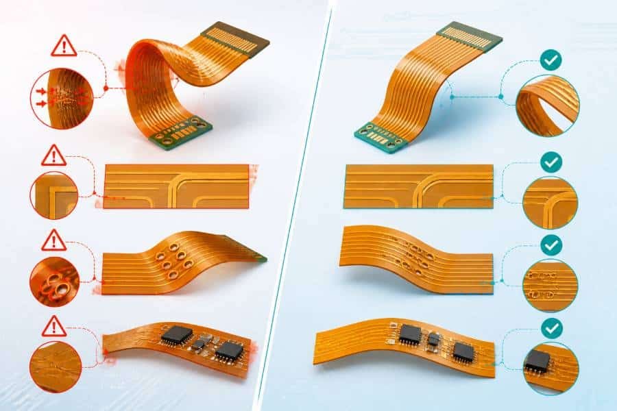
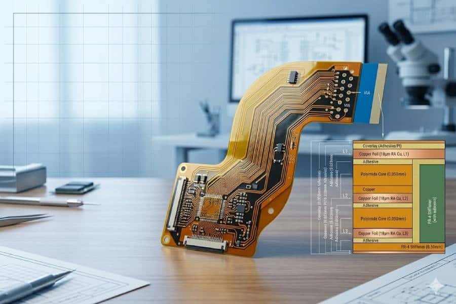
PCB Design

4 layer vs 6 layer pcb

4 Layer vs 6 Layer PCB: How to Choose the Right Stackup for Your Design

Choosing between a 4 layer and 6 layer PCB is often a trade‑off between performance, EMI risk, routing freedom, and budget. This guide walks you through real‑world use cases, key comparison points, and a simple checklist you can use to decide whether 4 layers are enough or it is time to step up to a 6 layer stackup.

4 Layer vs 6 Layer PCB: How to Choose the Right Stackup for Your Design Read More »

high frequency pcb solutions for satellite communication terminals

High Frequency PCB Solutions for Satellite Communication Terminals | Satellite Communication PCB Guide

Satellite communication terminals rely on specialized high frequency PCBs to route low‑loss RF signals, interface with antennas, and survive harsh thermal and mechanical conditions on the ground and in orbit. This guide explains how to choose materials, stackups, and layouts for a satellite communication PCB and high frequency PCB for satellite systems that deliver low loss, stable impedance, and long‑term reliability.

High Frequency PCB Solutions for Satellite Communication Terminals | Satellite Communication PCB Guide Read More »

high frequency pcbs in automotive radar and adas systems

High Frequency PCBs in Automotive Radar and ADAS Systems | Automotive Radar PCB Design Guide

Automotive radar PCB design sits at the heart of modern ADAS systems, where 77–79 GHz signals, harsh automotive environments, and strict safety targets all meet on a high frequency PCB. This guide explains how to choose materials, stackups, and layouts for automotive radar PCBs and high frequency PCBs for ADAS that are accurate, robust, and ready for mass production.

High Frequency PCBs in Automotive Radar and ADAS Systems | Automotive Radar PCB Design Guide Read More »

high frequency pcbs for 5g base stations and small cells design & manufacturing tips

High Frequency PCBs for 5G Base Stations and Small Cells | Design & Manufacturing Tips

High frequency PCBs are at the core of 5G macro base stations and small cells, where Sub‑6 and mmWave signals demand low loss, tight impedance control, and robust reliability in harsh outdoor environments. This guide shares practical design and manufacturing tips—from material and stackup choices to RF layout, thermal, and DFM checks—to help you turn 5G concepts into stable, high‑volume hardware.

High Frequency PCBs for 5G Base Stations and Small Cells | Design & Manufacturing Tips Read More »

Hybrid High Frequency PCBs: Combining Rogers and FR4 for RF and Digital Integration

Hybrid High Frequency PCBs: Combining Rogers and FR4 for RF and Digital Integration

Hybrid high frequency PCBs use Rogers for critical RF layers and FR4 for digital, control, and power layers in a single stackup. This article explains why and when to choose a hybrid design, shows common Rogers+FR4 stackup patterns, and shares practical layout and manufacturing guidelines so your RF and digital sections work together without blowing up the budget.

Hybrid High Frequency PCBs: Combining Rogers and FR4 for RF and Digital Integration Read More »

Scroll to Top