Table of Contents
Introduction: Why Multilayer PCB Stackup And Thickness Matter
In modern electronics, products are becoming smaller, lighter, faster and more integrated, yet they are expected to deliver more functionality, higher reliability and a longer service life. To meet these demands, designers increasingly rely on multilayer PCBs, where the layer stackup and overall board thickness play a critical role in the final performance of the product.
A PCB stackup describes the arrangement of copper layers and insulating layers in the board before layout starts. For a multilayer PCB, this usually includes signal layers, ground planes (GND planes) and power planes (PWR planes), separated and bonded together by core materials and prepregs. Beyond simply deciding how many layers you need, you must also carefully plan which layers carry which signals, how reference planes are placed, and how thick each dielectric layer should be.
A well‑designed multilayer stackup can significantly improve EMC/EMI performance, signal integrity and power integrity, while also helping to control impedance, crosstalk and noise. At the same time, the overall PCB thickness affects mechanical strength, connector compatibility, thermal performance and manufacturability. On the other hand, a poor stackup choice may lead to excessive EMI radiation, reflections, ringing and reliability issues, even if the schematic and layout rules look correct.
This guide will walk you through the basics of multilayer PCB stackup, explain the key factors that influence board thickness, and summarize standard thickness options from 4‑layer up to 14‑layer PCBs based on JHYPCB’s manufacturing experience. You will also find practical stackup examples, selection tips and design considerations that make it easier to choose the right configuration for your next project. If you are not sure which stackup and thickness are best for your design, our engineering team can review your requirements and propose optimized options before fabrication.
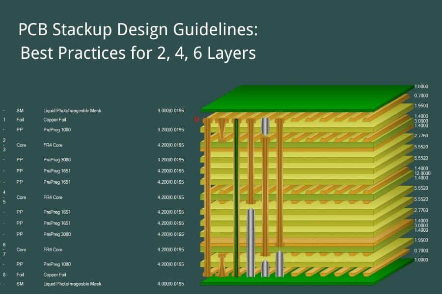
PCB Stackup Basics: Core, Prepreg And Copper Layers
A multilayer PCB stackup is much more than a simple count of copper layers – it is a carefully engineered sequence of copper and dielectric layers that determines how well your board can carry signals, distribute power and withstand mechanical stress. Before the PCB layout begins, the stackup defines where signal layers, ground planes and power planes will be placed, as well as what materials and thicknesses will be used between them.
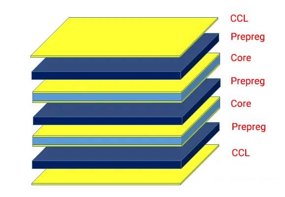
In a typical multilayer PCB, the main building blocks of the stackup are copper foils, core materials and prepregs. Core is a rigid, copper‑clad laminate (for example, FR‑4) that already has copper on both sides and provides the mechanical backbone of the board. Prepreg is a fiberglass fabric pre‑impregnated with resin, used to bond layers together during lamination and to build up the required dielectric thickness between copper layers. During the lamination process, multiple cores and prepregs are stacked with copper foils, then pressed and cured under high temperature and pressure to form a single solid board.
For most designs, a good stackup aims to keep the structure as symmetrical as possible around the center of the board. Symmetrical or “balanced” stackups help reduce warpage and internal stress, especially for high‑layer‑count or large‑size boards. A common approach is to mirror signal layers and plane layers around the middle of the stack, and to use similar core and prepreg combinations on both sides. This not only improves mechanical stability, but also makes impedance control and layer‑to‑layer matching easier for the PCB manufacturer.
Key Factors That Affect Multilayer PCB Thickness
When you design a multilayer PCB, the final board thickness is not chosen in isolation – it is the result of several electrical, mechanical and manufacturing constraints that must be balanced together. Understanding these factors helps you select a thickness that is both performance‑optimized and cost‑effective.
1. Number of Layers and Layer Arrangement
The most fundamental driver of PCB thickness is the total number of layers and how they are arranged as signal layers, ground planes and power planes. More layers usually mean more cores and more prepreg interfaces, which naturally increases the overall thickness. In addition, stackups with multiple reference planes (for controlled‑impedance and EMC performance) may require minimum dielectric spacing that further affects thickness.
2. Core and Prepreg Thickness Selection
The combined thickness of cores and prepregs is typically the largest contributor to total board thickness. Different FR‑4 core options and prepreg styles (for example 1080, 2116, 7628) come with specific nominal thicknesses and tolerances, and designers choose them based on:
- Required dielectric spacing for impedance control;
- Desired mechanical rigidity or flexibility;
- Lamination process constraints of the PCB manufacturer.
Thicker cores and more robust prepreg stacks lead to a thicker and stiffer board, while thinner dielectrics support compact designs but may tighten manufacturing tolerances.
3. Copper Thickness (Copper Weight)
Each copper layer adds to the total thickness of the PCB. Using heavier copper (for example 2 oz instead of 1 oz) increases the board thickness and can also influence the dielectric thickness required to meet a specific impedance target. High‑current power stages, wide power rails or high‑reliability applications often need thicker copper, so designers must account for this when calculating the overall stackup height.
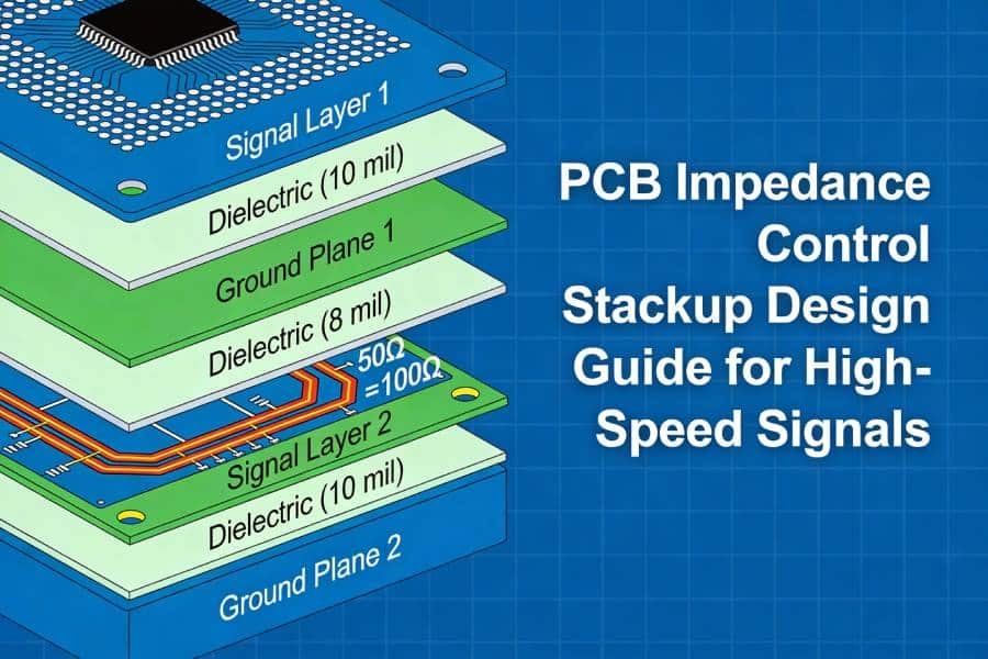
4. Impedance Control and High‑Speed Requirements
For high‑speed or RF designs, controlled‑impedance traces are often mandatory. The required impedance is determined by trace width, copper thickness, dielectric thickness and dielectric constant (Dk). To hit a specific impedance (for example 50 Ω single‑ended or 100 Ω differential), you may need to adjust the dielectric thickness between signal layers and their reference planes, which directly impacts the total board thickness and the choice of core/prepreg combinations.
5. Mechanical Strength and System‑Level Constraints
From a mechanical perspective, PCB thickness must fit within the product enclosure and meet stiffness or flexibility requirements. Thicker boards provide greater rigidity and durability, which is important in large panels, connector‑dense boards or harsh environments. Thinner boards are preferred where weight, space or flex are critical, such as wearables or compact IoT devices. At the same time, you must respect connector specifications, slot or card‑edge thickness requirements and any system‑level mechanical tolerances.
6. Thermal Performance and Reliability Considerations
Board thickness also influences thermal behavior and long‑term reliability. Thicker boards and heavier copper can help spread and conduct heat away from hot components, but may also increase thermal gradients through the stack. In high‑power or high‑temperature applications, material choice (for example high‑Tg FR‑4 or special high‑frequency laminates) and thickness planning are important to avoid delamination, warpage and via reliability issues.
7. Manufacturing Capabilities and Cost
Finally, the capabilities and standard practices of your PCB manufacturer strongly influence the practical range of thicknesses. Most fabricators have standard stackup constructions for common thicknesses (such as around 1.6 mm) and layer counts, which usually offer better cost, yield and lead time. Non‑standard thicknesses or exotic stackups may be possible, but they can require special materials, additional process steps and tighter process control, which increases cost. Early communication with your PCB supplier about available core/prepreg combinations, copper weights and thickness tolerances is essential to avoid redesign later in the project.
Standard Multilayer PCB Thickness Options (4‑Layer To 14‑Layer)
Selecting a standard board thickness is often the first practical decision when planning a multilayer PCB stackup. While the exact thickness depends on your layer count, materials and application, most designs fall within a relatively narrow range of industry‑proven FR‑4 options.
1. Typical Thickness Range For Common Layer Counts
For many applications, PCB manufacturers offer standardized thickness options that balance mechanical strength, manufacturability and cost:
- 4‑Layer PCBs
- Most common “standard” thickness around 1.6 mm (0.063″).
- Practical range often from about 1.0 mm up to 2.4 mm, depending on design needs and material selection.
- 6‑Layer PCBs
- Frequently built at 1.6 mm as well, especially for general‑purpose digital and industrial designs.
- Many fabricators also support thicker options (for example 2.0–2.4 mm) for higher layer counts or mechanically demanding boards.
- 8‑Layer And Above (8/10/12/14‑Layer)
- As the layer count increases, finished thickness commonly moves to 2.0 mm (0.079″) and above, to accommodate more cores, prepregs and possible heavier copper.
- Practical ranges for high‑layer‑count boards typically fall between about 1.6 mm and 3.0 mm, with specific values chosen based on signal integrity, mechanical and thermal requirements.
Across these layer counts, standard FR‑4 board thicknesses such as 0.8 mm, 1.0 mm, 1.2 mm, 1.6 mm and 2.0 mm are widely used because they align well with panel utilization, material availability and connector standards.
2. Overview Table: Standard Thickness Options By Layer Count
The table below summarizes typical finished thickness options for common multilayer configurations and their typical use cases.
| Layer Count | Typical Standard Thickness | Common Range | Typical Applications |
|---|---|---|---|
| 4‑Layer PCB | 1.6 mm (0.063″) | ~1.0–2.4 mm | Compact controllers, consumer & industrial boards |
| 6‑Layer PCB | 1.6 mm | ~1.6–2.4 mm | High‑speed digital, MCU + interfaces, control |
| 8‑Layer PCB | 2.0 mm (0.079″) | ~1.6–3.0 mm | Complex high‑speed, telecom, dense FPGA/BGA |
| 10‑Layer PCB | ≈2.0–2.4 mm | ~1.8–3.0 mm | Advanced networking, computing, backplanes |
| 12‑Layer PCB | ≈2.0–2.4 mm | ~2.0–3.0 mm | High‑density, multi‑interface embedded systems |
| 14‑Layer PCB | ≈2.4–3.0 mm | ~2.0–3.2 mm (or higher) | Very high‑speed, multi‑plane, complex SoC/FPGA |
These values are typical, not absolute limits. Many manufacturers can produce thinner or thicker versions of each layer count by adjusting core/prepreg combinations and copper weights, but staying close to standard thicknesses generally results in better cost and lead time.
3. How This Overview Connects To The Following Sections
In the next sections, we will look more closely at specific layer counts, starting with 4‑layer and 6‑layer PCBs, and discuss:
- Which finished thicknesses are most commonly used in real projects;
- Example stackup configurations for different applications;
- How to choose between options such as 0.8 mm, 1.0 mm, 1.2 mm, 1.6 mm and 2.0 mm in practice.
This will give you practical guidance for selecting a standard thickness that fits both your design requirements and your PCB manufacturer’s capabilities.
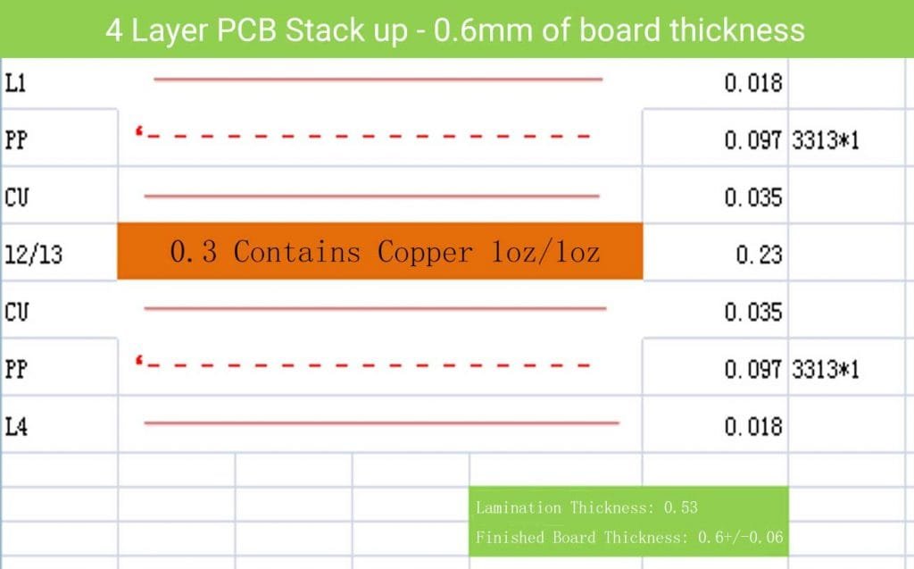
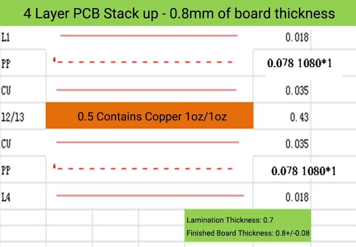
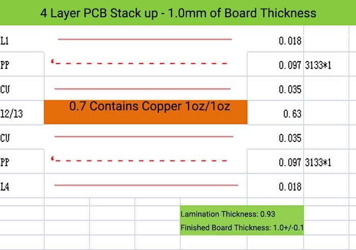
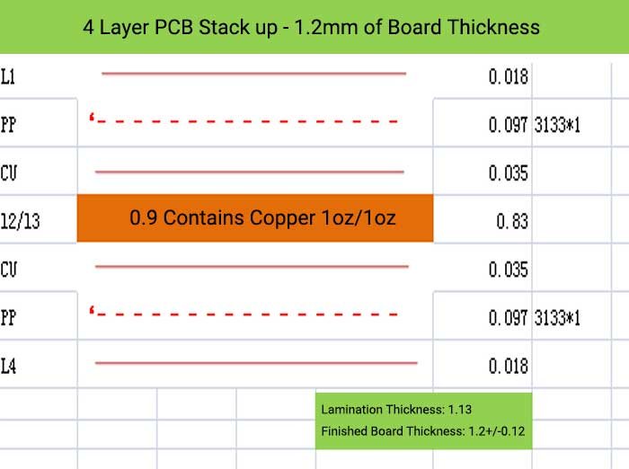
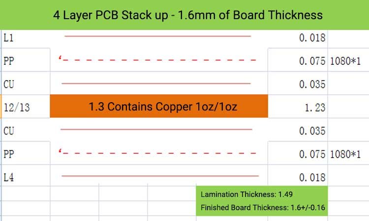
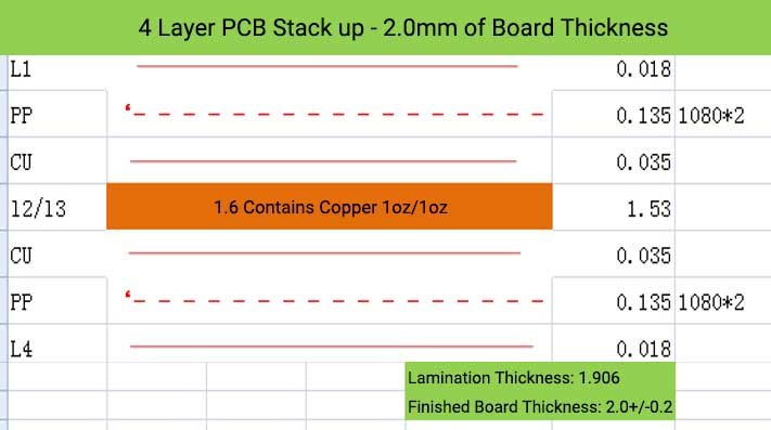
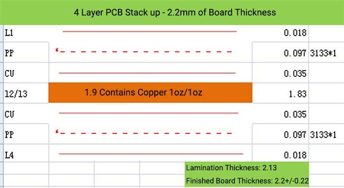
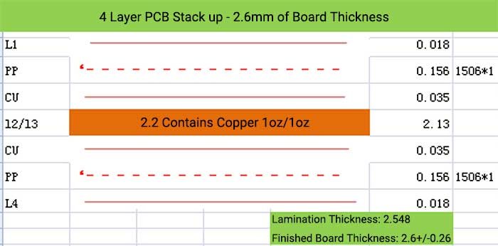
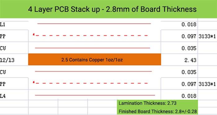
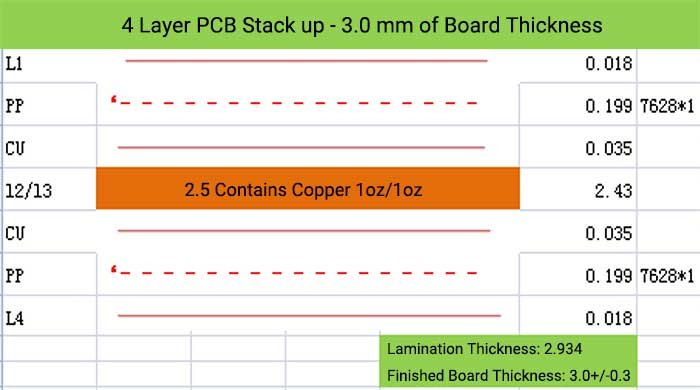
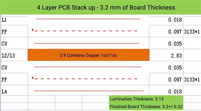
4‑Layer PCB Stackup And Standard Thickness Options
Typical 4‑Layer PCB Thicknesses
Among all multilayer configurations, 4‑layer PCBs are one of the most widely used choices for embedded systems, industrial controllers, consumer electronics and IoT devices. They provide a good balance between signal integrity, EMI performance and cost, while keeping the board structure relatively simple.
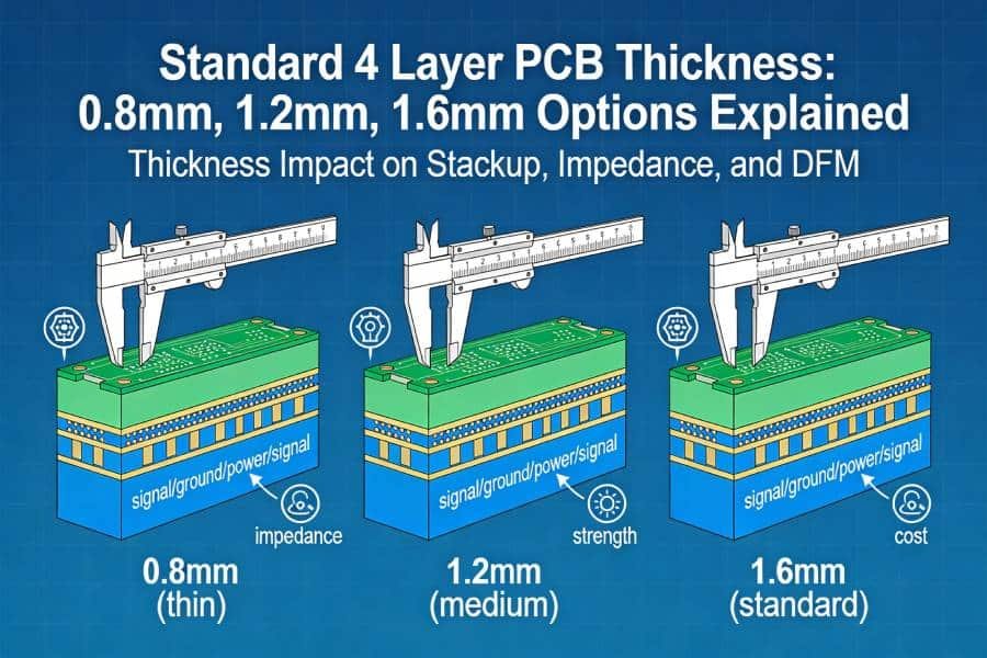
In FR‑4‑based designs, the most common standard finished thickness for a 4‑layer PCB is around 1.6 mm (0.063″). This thickness is compatible with a wide range of connectors, sockets and mechanical fixtures, and it fits well with standard material combinations that PCB manufacturers keep in stock.
However, 4‑layer boards are not limited to 1.6 mm. Many fabricators can also offer other standard thickness options, for example:
- 0.8 mm – for compact, lightweight and space‑constrained designs;
- 1.0 mm – a common choice when you need a thinner profile but still want reasonable rigidity;
- 1.2 mm – a compromise between thin form factor and mechanical strength;
- 1.6 mm – the industry‑standard option for general‑purpose applications;
- 2.0 mm and above – for boards that require extra stiffness or must match specific connector/card thickness.
When you plan a 4‑layer stackup, it helps to start from a standard thickness (such as 1.0 mm, 1.2 mm or 1.6 mm) and then work with your PCB supplier to fine‑tune the core and prepreg combination to meet your impedance and mechanical requirements.
Example 4‑Layer Stackup Configurations
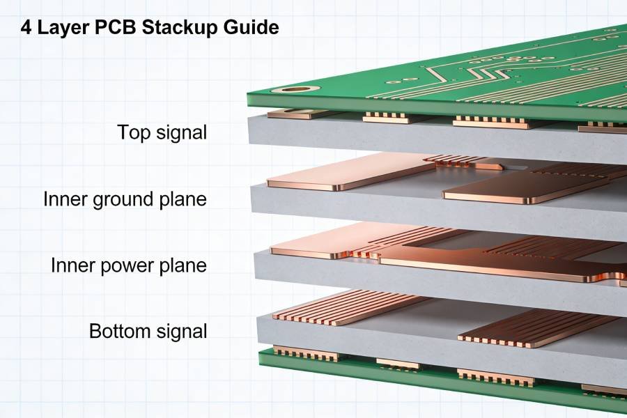
A typical 4‑layer PCB uses the following layer order:
- Layer 1 (Top Layer): Signal
- Layer 2 (Inner Layer 1): Ground plane (GND)
- Layer 3 (Inner Layer 2): Power plane (PWR) or mixed signal
- Layer 4 (Bottom Layer): Signal
This structure allows top and bottom signal layers to reference nearby planes, which helps control EMI and impedance, while the inner layers provide solid reference planes and stable power distribution.

Application Scenarios For Different 4‑Layer Thicknesses
Choosing the right 4‑layer PCB thickness depends on how the board will be used:
- 0.8–1.0 mm 4‑Layer PCBs
- Best suited for compact modules, wearables and dense IoT devices.
- Help reduce overall product height and weight, but result in a more flexible board that may need additional mechanical support.
- 1.2–1.6 mm 4‑Layer PCBs
- Common in industrial, automotive, power and control applications.
- Provide a good balance between stiffness, manufacturability and cost, making them a safe default choice for many designs.
- 2.0 mm And Thicker 4‑Layer PCBs
- Used when mechanical robustness is critical (for example large boards, card‑edge connectors, relay boards).
- Offer higher rigidity, but also increase weight and material cost, so they are typically selected only when required by the mechanical design or connector standard.
If you are not sure which 4‑layer stackup and thickness is best for your project, you can share your schematic, interface list or preliminary layout with our engineering team. Based on your signal speeds, power levels and mechanical constraints, we can recommend one or two optimized 4‑layer stackup options that balance performance, reliability and cost before you move into final layout and fabrication.
6‑Layer PCB Stackup And Standard Thickness Options
Typical 6‑Layer PCB Thicknesses
A 6‑layer PCB is often chosen when a 4‑layer board can no longer provide enough routing space, power distribution quality or EMI performance for modern high‑speed designs. It adds two extra layers compared to a 4‑layer PCB, which allows more controlled‑impedance routing and better separation of signal and plane layers.
For FR‑4‑based 6‑layer boards, a very common standard finished thickness is also around 1.6 mm (0.063″), especially for general‑purpose digital and industrial applications. Many manufacturers additionally support thicker options, such as 2.0 mm or 2.4 mm, when you need extra rigidity, more copper or must match specific connector or card‑edge specifications. In practice, the typical thickness range for 6‑layer PCBs is about 1.6–2.4 mm, although thinner or thicker constructions are possible with customized stackups.
When planning a 6‑layer design, it is usually efficient to start from your fabricator’s standard 1.6 mm or 2.0 mm constructions, then adjust core, prepreg and copper weight only if needed for special impedance, mechanical or thermal requirements.
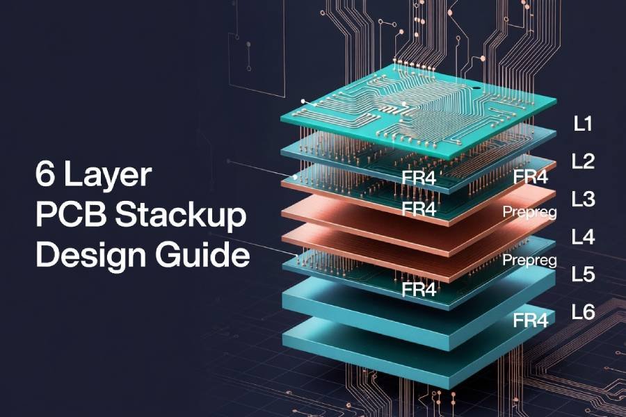
Example 6‑Layer Stackup Configurations
A typical 6‑layer PCB stackup aims to provide:
- Dedicated ground planes close to signal layers for good return paths and EMI control;
- At least one power plane for low‑impedance power distribution;
- Enough signal layers for dense routing and fan‑out of fine‑pitch BGAs.
One widely used 6‑layer structure looks like this:
- L1 – Top Layer: High‑speed / critical signals
- L2 – Inner Layer 1: Ground plane (GND)
- L3 – Inner Layer 2: Power plane (PWR) or mixed signal
- L4 – Inner Layer 3: Inner signal layer
- L5 – Inner Layer 4: Ground plane (GND)
- L6 – Bottom Layer: General or secondary signals
This arrangement allows outer signal layers (L1, L6) to be closely referenced to ground planes on L2 and L5, which helps maintain controlled impedance and reduce EMI. The inner planes (L2, L3, L5) provide solid reference for high‑speed traces and stable power distribution, while L4 offers additional routing capacity for dense designs.
Recommended Use Cases For 6‑Layer PCBs
Compared with 4‑layer boards, 6‑layer PCBs are particularly attractive when your design includes:
- Multiple high‑speed interfaces (such as USB 3.x, HDMI, DisplayPort, PCIe, Gigabit Ethernet, DDR memory);
- High‑pin‑count BGA packages that require extra routing channels;
- Strict EMI/EMC requirements, where additional ground planes help shield sensitive signals;
- Mixed‑signal architectures, where analog and digital domains need better separation;
- Higher current levels or power density, which benefit from dedicated power and ground planes.
Typical application areas for 6‑layer PCBs include networking and communication equipment, industrial control systems, automotive electronics, high‑performance embedded modules and RF/microwave assemblies. In many of these designs, a carefully planned SIG/GND/PWR/SIG/GND/SIG‑style stackup can significantly improve signal integrity, power integrity and EMC robustness without jumping straight to more expensive 8‑layer or 10‑layer boards.
If you are upgrading from a 4‑layer design and are not sure how to migrate your layout to 6 layers, you can share your existing PCB files, interface list and problem areas (such as EMI, crosstalk or routing congestion) with our engineering team. Based on that, we can propose one or more 6‑layer stackup options and suggest which signals and planes to place on each layer to achieve a better balance of performance, reliability and cost.
8‑Layer PCB Stackup Overview And Standard Thickness
Typical 8‑Layer PCB Thicknesses
An 8‑layer PCB is often selected for complex, high‑speed and high‑density designs, where 4‑layer or 6‑layer boards can no longer provide enough routing space or sufficient separation between noisy and sensitive signals. With eight layers available, designers can allocate multiple signal layers and reference planes, achieving better EMI shielding, signal integrity and power integrity in a relatively compact form factor.
For FR‑4‑based 8‑layer stackups, typical finished thickness values usually fall between about 1.6 mm and 2.4 mm. Many standard 8‑layer constructions are built close to 1.6 mm (0.062″) or around 2.0–2.4 mm (0.079–0.093″), depending on the chosen core/prepreg combinations, dielectric spacing and copper weights. Thinner 8‑layer HDI boards are technically possible—even below 1.0 mm—but they generally require special materials, finer processing and higher cost, so they are reserved for very compact or advanced applications.
When you plan an 8‑layer design, it is usually recommended to start from standard thickness options (such as 1.6 mm or about 2.0 mm) offered by your PCB manufacturer, and then adjust dielectric thicknesses and material choices only as needed to meet your impedance and mechanical targets.
Typical 8‑Layer Stackup Concepts
With eight layers, there are many possible stackup arrangements, but most high‑speed designs follow a few common principles:
- Place high‑speed signal layers directly adjacent to solid ground planes to ensure short return paths and controlled impedance.
- Use inner layers for additional ground planes and power planes, improving shielding and lowering power distribution impedance.
- Keep the stackup symmetrical around the center to minimize warpage and internal stress.
A representative 8‑layer concept for high‑speed digital applications might look like this:
- L1 – Top Layer: High‑speed or critical signals
- L2 – Ground Plane (GND)
- L3 – Inner Signal Layer (often lower‑speed or secondary high‑speed)
- L4 – Power Plane (PWR)
- L5 – Power or Ground Plane (PWR/GND)
- L6 – Inner Signal Layer (often high‑speed or differential pairs)
- L7 – Ground Plane (GND)
- L8 – Bottom Layer: General or auxiliary signals
This kind of structure allows you to sandwich critical signal layers between reference planes, improving EMI shielding and crosstalk control, while central power/ground planes provide stable reference and low‑impedance power delivery.
When To Consider 8‑Layer (And Higher‑Layer‑Count) PCBs
Moving from 6 layers to 8 layers is usually justified when your design requires:
- Multiple very high‑speed interfaces (for example multi‑lane SerDes, high‑bandwidth memory buses, high‑speed backplane links);
- Extensive BGA fan‑out for large FPGAs, SoCs or high‑pin‑count processors;
- Stricter EMC/EMI performance, where additional ground planes and shielding are needed;
- Complex mixed‑signal or RF front‑ends, where noisy digital and sensitive analog/RF sections must be carefully isolated.
Beyond 8 layers, 10‑layer, 12‑layer and 14‑layer PCBs are typically used in high‑end networking, telecommunications, computing and instrumentation equipment, where designers need even more routing layers and separate planes for multiple power domains and high‑speed channels. For these high‑layer‑count boards, finished thickness often ranges from about 2.0 mm to 3.0 mm or more, depending on layer count, copper weight and mechanical requirements.
If you are unsure whether your design really needs an 8‑layer or higher‑layer‑count PCB, you can share your schematic, interface list, rough placement and main design challenges (such as EMI issues or routing congestion) with our engineering team. We can help you evaluate whether a well‑optimized 6‑layer stackup is sufficient, or if moving to 8 layers or more will provide clear benefits in terms of signal integrity, EMC and overall layout efficiency.
10‑Layer PCB Stackup Overview And Standard Thickness
Typical 10‑Layer PCB Thicknesses
A 10‑layer PCB is widely used in high‑speed, high‑density and high‑reliability electronic systems, where designers need more routing freedom and better control over signal integrity, power integrity and EMC than 6‑layer or 8‑layer boards can provide. With ten layers available, it becomes much easier to separate noisy and sensitive circuits, dedicate multiple planes to power and ground, and still keep enough signal layers for dense BGA fan‑out and complex interfaces.
In practice, many 10‑layer FR‑4 stackups are built close to standard board thickness values such as about 1.6 mm (0.062″) or around 2.0–2.4 mm (0.079–0.093″), depending on the chosen core/prepreg combination and copper weight. Manufacturers often provide standard 10‑layer stackup options at these thicknesses to balance cost, manufacturability and performance. Thicker 10‑layer designs (approaching 3.0 mm or more) are also possible for very rigid or high‑power boards, but they typically increase material usage and cost.
When specifying a 10‑layer stackup, it is usually efficient to start from your PCB supplier’s standard 0.062″ or 0.093″ 10‑layer constructions, then fine‑tune dielectric thicknesses only where necessary to meet critical impedance or mechanical requirements.
Typical 10‑Layer Stackup Concepts
A well‑designed 10‑layer stackup normally follows the principle of alternating signal layers with reference planes (power/ground) to minimize interference and maintain stable impedance. Compared with lower‑layer configurations, it allows more dedicated ground planes, more separate power domains, and additional inner signal layers for dense routing.
One common 10‑layer concept for high‑speed digital designs looks like this (from top to bottom):
- L1 – Top Layer: High‑speed or critical signals, components and connectors
- L2 – Ground Plane (GND): Solid reference plane for L1
- L3 – Inner Signal Layer: High‑speed or dense routing
- L4 – Ground Plane (GND): Reference for L3 and shielding for inner layers
- L5 – Power Plane (PWR): Main power distribution or split power regions
- L6 – Power Plane / Ground Plane (PWR/GND): Additional power domain or ground
- L7 – Ground Plane (GND): Reference for L8 and inner signals
- L8 – Inner Signal Layer: High‑speed or secondary routing
- L9 – Ground Plane (GND): Solid reference for L8
- L10 – Bottom Layer: General or secondary signals, connectors, test pads
This type of structure:
- Places critical signal layers (L1, L3, L8, L10) next to solid ground planes, ensuring short return paths and good impedance control;
- Uses multiple ground planes (L2, L4, L7, L9) to improve EMI shielding, reduce crosstalk and stabilize reference potential;
- Allocates two central power/ground planes (L5, L6) for low‑impedance power distribution and decoupling.
Typical Applications For 10‑Layer PCBs
Because of their high routing capacity and strong EMC performance, 10‑layer PCBs are common in advanced electronic systems such as:
- Telecommunications and networking equipment – high‑port‑count switches, routers, base stations, backplanes;
- High‑performance computing and server boards – processor modules, memory subsystems, high‑speed interconnects;
- Industrial and medical equipment – complex control systems, instrumentation, imaging and monitoring devices;
- High‑end embedded systems – FPGA/SoC modules, advanced automotive ECUs, radar and signal‑processing units.
In these applications, designers benefit from the ability to:
- Route numerous high‑speed differential pairs while maintaining tight impedance control;
- Use multiple ground planes to significantly improve signal integrity and EMC;
- Separate noisy digital sections from sensitive analog/RF or power‑supply areas more effectively;
- Support high pin‑count BGAs and dense component placement without excessive via congestion.
If you are evaluating whether your project should move to a 10‑layer stackup, you can share your interface requirements, BGA pin‑maps and current layout challenges with our engineering team. We can help you compare optimized 8‑layer and 10‑layer options, and recommend a layer arrangement and finished thickness that provide the right balance between performance, reliability, cost and manufacturability.
12‑Layer PCB Stackup Overview And Standard Thickness
Typical 12‑Layer PCB Thicknesses
A 12‑layer PCB is usually selected for very complex, high‑speed and high‑density electronic systems, where designers must combine multiple high‑speed interfaces, several power domains and sensitive analog/RF circuits on a single board. With twelve copper layers available, it becomes possible to allocate numerous signal layers and multiple dedicated power and ground planes, while still maintaining compact overall dimensions.
In FR‑4‑based manufacturing, typical finished thickness values for 12‑layer PCBs commonly fall in the range of about 1.6 mm to 2.4 mm, and many fabricators standardize around approximately 1.6 mm (0.062″) or 2.0–2.4 mm (0.079–0.093″). Higher‑layer‑count boards like 12‑layer often require thinner dielectric layers to stay near these standard thicknesses, but some manufacturers also support thicker 12‑layer options (around 2.4–3.0 mm) for special mechanical or high‑power requirements.
When you specify a 12‑layer stackup, it is generally recommended to start from standard thickness options provided by your PCB supplier (for example 1.6 mm or ≈2.0 mm), and then fine‑tune the core and prepreg thicknesses to achieve the desired combination of impedance, mechanical strength and thermal performance.
Typical 12‑Layer Stackup Concepts
A 12‑layer PCB stackup typically alternates signal layers with ground and power planes to maximize signal quality and isolation. Compared with lower‑layer boards, it allows:
- More high‑speed signal layers to support multiple fast interfaces and dense BGA fan‑out;
- Several ground planes to shield critical traces and control return paths;
- Multiple power planes for different voltage rails and current levels.
A representative 12‑layer concept for high‑speed designs might look like this:
- L1 – Top Layer: Components and mixed‑speed signals
- L2 – High‑Speed Signal Layer: Critical high‑speed or differential pairs
- L3 – Ground Plane (GND): Solid reference for L2 and shielding for inner layers
- L4 – Inner Signal Layer: High‑speed or dense routing
- L5 – Ground Plane (GND): Additional reference and shielding
- L6 – Power Plane (PWR): Main power distribution or split rails
- L7 – Power Plane / Ground Plane (PWR/GND): Extra power domain or ground
- L8 – Ground Plane (GND): Reference for inner signals
- L9 – Inner Signal Layer: High‑speed or sensitive signals
- L10 – Ground Plane (GND): Reference for L9
- L11 – Inner Signal Layer: Lower‑speed or control signals
- L12 – Bottom Layer: Components, connectors, test pads or general routing
Typical Applications For 12‑Layer PCBs
Because of their high routing density, strong isolation capability and robust EMC performance, 12‑layer PCBs are widely used in advanced systems such as:
- Telecommunications and networking infrastructure – core routers, switches, high‑speed optical modules;
- Data center and high‑performance computing hardware – CPU/GPU/FPGA boards, accelerator cards, storage controllers;
- Advanced automotive, aerospace and defense electronics – radar, ADAS controllers, avionics modules;
- Complex mixed‑signal and RF front‑end systems – where high‑speed digital, sensitive analog and RF blocks must coexist in a compact footprint.
In these designs, a 12‑layer stackup helps engineers to:
- Route many impedance‑controlled high‑speed channels while maintaining strict signal integrity;
- Use multiple ground planes to minimize EMI, crosstalk and noise coupling between different functional blocks;
- Provide stable, low‑impedance power distribution for complex SoCs, FPGAs and high‑current loads;
- Achieve a compact, mechanically robust board that fits into tight enclosures without sacrificing performance.
If you are considering a 12‑layer PCB for your project, you can share your system block diagram, interface list, estimated layer usage and key constraints with our engineering team. Based on this information, we can recommend a practical 12‑layer stackup and finished thickness that align with your EMC, signal integrity, power and mechanical requirements, and verify that the design fits within our standard manufacturing capabilities.
14‑Layer PCB Stackup Overview And Standard Thickness
Typical 14‑Layer PCB Thicknesses
A 14‑layer PCB is designed for very high‑density, high‑speed and high‑reliability systems, where multiple high‑speed interfaces, complex power networks and sensitive analog/RF circuits must coexist on one board. With fourteen copper layers, designers can allocate several dedicated signal layers, multiple ground planes and multiple power planes, achieving strong signal integrity and EMC performance in a compact footprint.
In FR‑4‑based production, typical finished thicknesses for 14‑layer PCBs usually fall in the range of about 2.0 mm to 3.0 mm, depending on the chosen core/prepreg stack and copper weights. Many real‑world 14‑layer designs target around 2.4–2.8 mm to balance mechanical rigidity, via aspect ratio and material cost, though thinner or thicker versions are possible with customized constructions. High‑density HDI 14‑layer boards may use very thin dielectrics and microvias, but they generally require advanced processes and tighter manufacturing tolerances.
When defining a 14‑layer stackup, it is important to coordinate early with your PCB manufacturer about available standard 14‑layer thickness options and maximum aspect ratio / via structures (through‑hole, blind/buried, stacked microvias) to ensure that the design remains manufacturable and cost‑effective.
Typical 14‑Layer Stackup Concepts
A 14‑layer PCB stackup typically alternates signal, ground and power layers in a way that:
- Keeps most high‑speed signal layers tightly coupled to adjacent ground planes;
- Provides multiple solid ground planes for shielding and low‑noise return paths;
- Allocates several power planes for different voltage rails and current levels;
- Maintains as much symmetry as possible to minimize warpage and internal stress.
A representative 14‑layer concept for high‑speed digital/telecom applications might look like this:
- L1 – Top Layer: Components and high‑speed signals
- L2 – Ground Plane (GND): Reference for L1
- L3 – High‑Speed Signal Layer: Critical differential pairs or memory buses
- L4 – Ground Plane (GND): Reference for L3 and shield for inner layers
- L5 – Inner Signal Layer: Dense routing, often high‑speed
- L6 – Power Plane (PWR): Main power distribution or split rails
- L7 – Ground Plane (GND): Central reference plane
- L8 – Power Plane (PWR): Additional power domains or high‑current rails
- L9 – Inner Signal Layer: Sensitive or high‑speed signals
- L10 – Ground Plane (GND): Reference for L9
- L11 – Inner Signal Layer: Mixed or lower‑speed signals
- L12 – Ground Plane (GND): Reference for L11
- L13 – Inner Signal Layer: General routing, fan‑out or control
- L14 – Bottom Layer: Components, connectors, test pads, auxiliary signals
Typical Applications For 14‑Layer PCBs
Thanks to their very high routing density and strong EMC capability, 14‑layer PCBs are widely used in demanding applications such as:
- Advanced communication systems – 5G base stations, high‑speed routers, core network equipment;
- Data center and server hardware – file servers, storage arrays, high‑speed backplanes and switching fabrics;
- High‑performance computing and graphics – CPU/GPU/FPGA motherboards, accelerator and interface cards;
- Industrial, aerospace and medical equipment – complex control units, test instruments, imaging and monitoring systems;
- Other high‑density, high‑speed electronics – HDMI and high‑bandwidth video systems, RF front‑ends, signal‑processing modules.
In these scenarios, a 14‑layer stackup helps designers to:
- Route a large number of impedance‑controlled high‑speed signals while keeping crosstalk and EMI under control;
- Use multiple ground planes to ensure clean return paths and robust isolation between digital, analog and RF domains;
- Provide wide, low‑impedance power planes for high‑current loads and multiple voltage rails;
- Integrate very high‑pin‑count BGAs and dense components without excessive via congestion.
If you are considering a 14‑layer PCB for your next project, you can share your system architecture, interface map, target data rates and mechanical constraints with our engineering team. We can help you determine whether a 12‑layer configuration is sufficient or whether a 14‑layer stackup will provide clear benefits, and then recommend a practical 14‑layer stackup and thickness that aligns with our manufacturing capabilities and reliability requirements.
How To Choose The Right Multilayer PCB Stackup And Thickness
Selecting the right multilayer PCB stackup and finished thickness is a balancing act between electrical performance, mechanical requirements, manufacturability and cost. A structured decision process helps you avoid late design changes and ensures that your PCB can be produced reliably.
Step‑By‑Step Selection Process
Step 1 – Define System And Interface Requirements
Start by listing the main functions and interfaces of your design:
- High‑speed interfaces (for example USB 3.x, HDMI, PCIe, Ethernet, DDR, SerDes);
- Sensitive analog/RF sections and precision measurement circuits;
- Power levels, current paths and number of voltage rails;
- Mechanical constraints such as maximum PCB thickness, board size and connector type.
This high‑level view will guide how many signal layers and reference planes you are likely to need.
Step 2 – Choose An Initial Layer Count
Based on complexity, pick an initial layer count as a starting point:
- 4 layers – compact controllers, simpler digital/analog designs;
- 6 layers – higher routing density, better EMC, multiple interfaces;
- 8 layers and above – complex high‑speed, multiple power domains, high‑pin‑count BGAs.
If you already know you must support several high‑speed buses, dense BGAs or strict EMC targets, start from 6 or 8 layers rather than trying to force everything into 4 layers.
Step 3 – Identify Controlled‑Impedance Requirements
List all signals that need controlled impedance (for example 50 Ω single‑ended, 90/100 Ω differential). For these signals, you must ensure that:
- Each high‑speed layer is adjacent to a solid ground plane;
- The dielectric thickness and material support the target impedance with practical trace widths;
- There is enough layer space to route all critical pairs with proper spacing and reference planes.
At this stage, you can roughly define which layers will be signal layers and which will be ground or power planes in your stackup concept.
Step 4 – Select A Standard Board Thickness Range
Choose a standard finished thickness that fits your mechanical and connector constraints, typically from common FR‑4 values such as 0.8 mm, 1.0 mm, 1.2 mm, 1.6 mm or 2.0 mm+. Consider:
- Product height and weight limitations;
- Required rigidity or flexibility of the board;
- Card‑edge or connector specifications that dictate a specific thickness (for example 1.6 mm);
- Typical standard thicknesses your PCB manufacturer recommends for the chosen layer count.
Whenever possible, stay close to your fabricator’s standard thickness options, as this usually leads to lower cost and shorter lead time.
Step 5 – Plan The Preliminary Stackup (Signal/Plane Arrangement)
Using your chosen layer count and thickness range, sketch a preliminary layer order:
- Place high‑speed signal layers adjacent to ground planes;
- Allocate enough ground planes for shielding and clean return paths;
- Assign power planes close to ground planes to form low‑impedance power distribution;
- Keep the overall structure as symmetrical as possible to minimize warpage.
At this stage, you do not need exact dielectric thickness values, but you should have a clear picture of which layer does what (SIG / GND / PWR) and how many cores and prepregs will be used.
Step 6 – Refine Core/Prepreg And Impedance Details With Your PCB Supplier
Once you have a draft stackup, share it with your PCB manufacturer together with your impedance targets and copper weights. Ask them to:
- Recommend specific core and prepreg combinations that fit your target thickness;
- Provide impedance calculations (or an impedance‑controlled stackup table) for your critical trace widths;
- Confirm manufacturing limits (minimum trace/space, via sizes, aspect ratios) for your chosen stackup.
This step ensures that your theoretical stackup can be manufactured reliably and meets both electrical and mechanical requirements.
Step 7 – Finalize The Stackup In Your Design Documentation
After you and your PCB supplier agree on the final stackup:
- Document the complete stackup table (layer names, copper weight, dielectric materials and thicknesses) in your fabrication drawing;
- Include controlled‑impedance requirements and tolerances;
- Make sure your PCB design tools (layer stack manager) use the same stackup definition.
Providing clear stackup information helps avoid misunderstandings and ensures that production PCBs match the performance characteristics you designed for.
Design Tips For Better EMC, SI And Manufacturability
To get the most out of your chosen stackup and thickness, keep the following best practices in mind:
- Prioritize Ground Planes
Use multiple, solid ground planes whenever possible. They provide low‑impedance return paths, reduce loop area, and improve EMI and signal integrity. - Keep Stackup Symmetrical
Aim for a balanced stackup around the center line of the board (similar layer counts and material thickness on both sides). This reduces warpage and internal stress during fabrication and assembly. - Minimize Dielectric Variation For Impedance‑Controlled Layers
Work with your manufacturer to use consistent dielectric thickness and stable materials (Dk/Df) around critical high‑speed layers, which makes impedance control more repeatable. - Use Standard Thicknesses And Materials When Possible
Whenever your design permits, choose standard FR‑4 thicknesses and copper weights. Non‑standard options can increase cost and lead time, and may require additional process adjustments. - Consider Via Structures Early
For higher‑layer‑count boards (8+ layers), decide early whether you need through‑hole only, blind/buried vias or HDI microvias, as this affects stackup design, thickness and manufacturing complexity. - Engage Your PCB Manufacturer Early
Early communication with your PCB supplier about layer count, thickness range, impedance targets and special requirements can prevent costly redesign later and often leads to a more optimized stackup overall.
Work With JHYPCB To Optimize Your Stackup And Thickness
Choosing the right multilayer PCB stackup and thickness can be challenging, especially when you are dealing with high‑speed signals, multiple power rails and strict EMC requirements. To make this process easier, the JHYPCB engineering team can support you from the early design stage through to volume production.
If you are not sure which layer count, stackup structure or finished thickness is best for your project, you can simply share:
- Your schematic or block diagram;
- A list of key interfaces (for example DDR, USB, Ethernet, PCIe, RF, high‑current power rails);
- Any special requirements (controlled impedance, target thickness, connector type, mechanical limits);
- Optional: a preliminary PCB layout or placement file if available.
Based on this information, our engineers can:
- Propose one or two optimized stackup options (including layer usage, copper weights and dielectric thicknesses) that fit your design goals and our standard manufacturing capabilities;
- Provide impedance‑controlled stackup recommendations for your critical high‑speed nets;
- Perform a DFM review to check manufacturability and highlight potential issues before you release the final Gerber files.
To get started, you can:
- Send your Gerber files, stackup ideas or design requirements to our team via sales@pcbjhy.com; or
- Submit your project details through the online quote / inquiry form on our website and indicate that you need stackup and thickness suggestions.
Our goal is to help you choose a reliable, cost‑effective multilayer PCB stackup that works well in manufacturing and delivers the electrical and mechanical performance your product requires.