Table of Contents
Intro
When you start routing high‑speed interfaces or RF sections, it is tempting to think of controlled impedance as something you can “fix later” with a line width calculator. In reality, the most important decisions that determine whether your impedance targets are achievable are made much earlier, when you define the PCB stackup and choose materials.
A good stackup gives your traces the right environment: stable dielectric properties, predictable thickness between signal layers and reference planes, and enough routing room to hit the required line widths and spacing.
A poor stackup, on the other hand, can force you into line widths that are too narrow to manufacture reliably, or into compromises that increase loss, crosstalk and EMI problems.
This guide explains the key stackup parameters that influence controlled impedance, compares common microstrip and stripline structures and walks through practical examples you can adapt to your own high‑speed designs. It also shows how to collaborate with your PCB manufacturer so that the stackup you design on paper can be implemented consistently on the shop floor.
For a practical overview of how stackup decisions translate into real production, you can also review our impedance control PCB fabrication capabilities.
Why stackup is critical for controlled impedance
From an impedance point of view, the PCB stackup defines almost everything the signal “sees” as it travels along a trace: the dielectric constant and thickness of the materials around it, the copper thickness and the position of the reference planes.
Trace geometry is still important, but without a well‑defined stackup, line width and spacing values from any calculator are just theoretical numbers that may not match the realities of fabrication.
Different stackup choices directly affect several aspects of your design. Thinner dielectrics and closer reference planes can help you reach a target impedance with wider traces, which may improve manufacturability and current‑carrying capacity.
Thicker dielectrics or higher‑Dk materials will require narrower traces for the same impedance, which can increase loss and make it harder to maintain consistent geometry across the panel.
Stackup decisions also influence EMI and crosstalk. Well‑placed ground planes under high‑speed layers provide a clear return path and allow you to control impedance while containing fields close to the board, which reduces radiation and coupling between adjacent routes.
If high‑speed signals are forced to cross plane splits or share layers with noisy power structures because of a weak stackup, you can end up with both impedance discontinuities and avoidable signal integrity problems, even if your line widths look correct in the layout tool.
Key parameters that influence PCB impedance
Dielectric constant (Dk) and loss tangent
The dielectric constant of your PCB laminate determines how strongly the electric field between a trace and its reference plane is concentrated in the material, which directly affects both characteristic impedance and signal velocity.
Standard FR‑4 materials typically have a higher and less tightly controlled Dk than dedicated high‑frequency laminates, so their impedance can vary more over temperature, frequency and lot‑to‑lot changes.
Loss tangent, sometimes called dissipation factor, tells you how much signal energy is converted to heat as it propagates through the dielectric.
At low to moderate data rates, this loss may be acceptable, but at very high frequencies or over long trace lengths it can significantly shrink the eye diagram and increase jitter, even if the nominal impedance is correct.
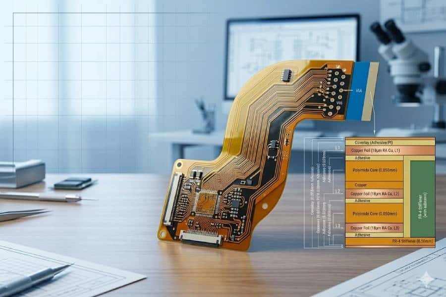
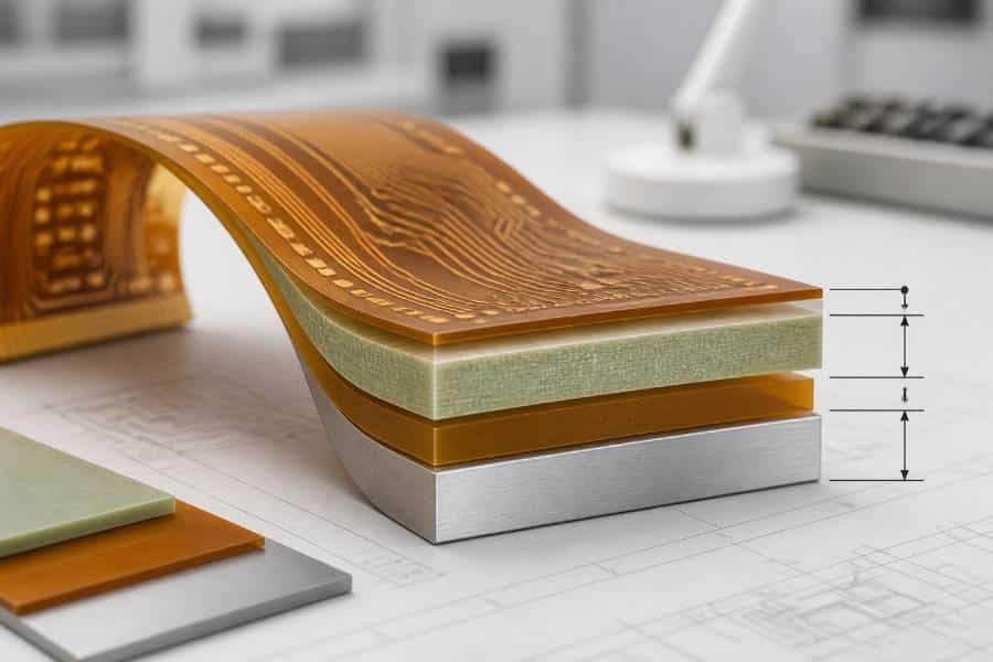
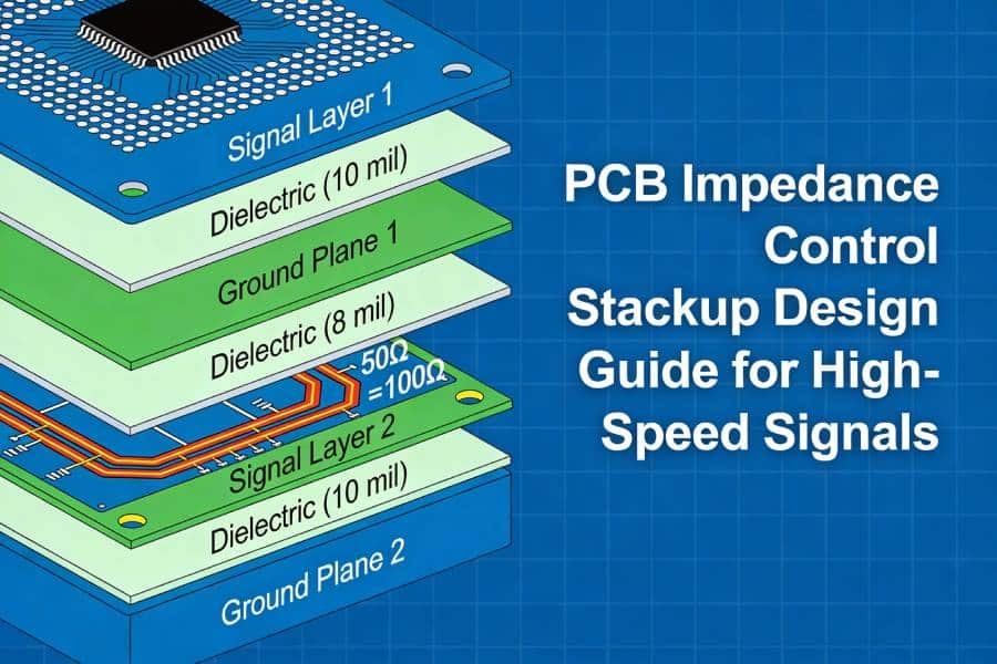
Dielectric thickness between signal and reference planes
The thickness of the dielectric between a signal layer and its reference plane is one of the main levers you and your PCB manufacturer can use to hit a target impedance.
For a given material and trace geometry, bringing the reference plane closer to the trace (thinner dielectric) lowers the impedance and allows you to use wider traces for the same target value.
Conversely, increasing the dielectric thickness raises the impedance for a given line width, which may force you into very narrow traces to reach common targets such as 50 Ω or 100 Ω.
Those narrow traces can be harder to manufacture consistently, more sensitive to etching variations and more prone to increased resistance and heating, especially on longer runs.
Copper thickness and trace width/spacing
Copper thickness also plays a role in controlled impedance. Thicker copper effectively increases the cross‑section of a trace and slightly changes its electromagnetic field distribution, which alters the impedance for a given line width.
In practice, inner layers are often built with thinner copper weights than outer layers, which affects both the achievable impedance and the minimum manufacturable trace geometry on each layer.
Trace width and spacing are the parameters designers most often adjust in impedance calculators, but they cannot be chosen in isolation. The values you obtain must be compatible with the manufacturer’s minimum line width, spacing and etch‑tolerance capabilities on the specific layer and copper weight you intend to use.
If your calculator suggests a geometry that is on the edge of what the process can reliably produce, a small change in etch rate or registration may push the actual impedance outside your tolerance window.
Reference planes and return paths
Reference planes are more than just copper shapes that happen to sit under a signal layer; they provide the return path that closes the loop for high‑frequency currents and help define a stable impedance environment for your traces.
A solid, continuous ground plane directly under a high‑speed signal layer makes it much easier to achieve consistent impedance, low loop inductance and predictable coupling between adjacent routes.
Problems arise when high‑speed signals have to cross plane splits, move between layers with different reference planes or share space with noisy power structures. Each of these situations can create localized impedance discontinuities and force return currents to take longer, more inductive paths.
Good stackup planning ensures that critical controlled‑impedance routes always have a clear, closely coupled reference plane and that any necessary transitions between planes are handled with appropriate stitching vias and layout constraints.

Common stackup structures for controlled impedance
Microstrip vs embedded microstrip
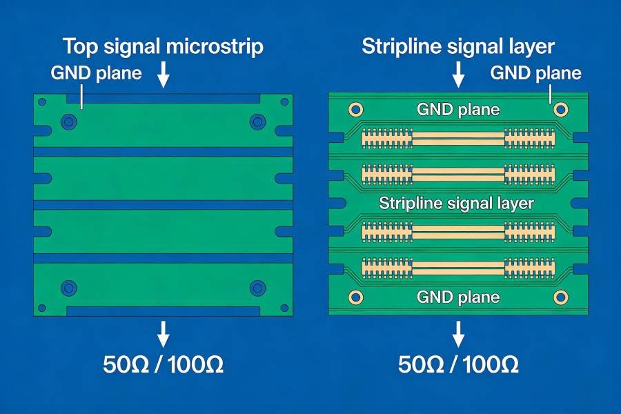
In many cost‑sensitive high‑speed designs, at least some controlled impedance traces are routed as microstrips on the outer layers of the PCB. A classic microstrip has air on one side of the trace and a dielectric plus reference plane on the other, which makes it relatively easy to access for probing and rework.
Because part of the field is in air, microstrips typically require wider traces than buried structures for the same impedance, which can be an advantage when you want to avoid pushing minimum line widths too far.
Embedded microstrips use a similar principle but place the trace just under the outer surface, covered by a thin dielectric layer while still referencing a nearby plane. This can improve environmental protection and allow for solder mask‑defined features while keeping the impedance behavior close to that of a standard microstrip.
Both variants are common in 4‑layer boards where top‑layer high‑speed routes reference a solid ground plane on the second layer, providing a straightforward path to 50 Ω single‑ended and 100 Ω differential structures.
Symmetric stripline and dual‑stripline
For more complex multilayer boards, symmetric stripline structures are often used for critical controlled‑impedance routes. In a symmetric stripline, the signal trace is buried between two reference planes within the dielectric, which provides good shielding, more consistent impedance and reduced sensitivity to external environmental changes.
Because all of the field is confined within the dielectric, stripline traces for a given impedance are usually narrower than microstrips, and they can be more sensitive to variations in dielectric thickness and material properties.
Dual‑stripline arrangements place two signal layers adjacent to the same pair of reference planes, such as a stackup where L3 and L4 are both signals sandwiched between ground planes on L2 and L5. This can increase routing density for controlled‑impedance traces while keeping return paths short and well defined.
However, dual‑stripline requires careful attention to spacing between layers and between adjacent traces to manage crosstalk, so it is important to coordinate line geometries and clearances with your PCB manufacturer’s capabilities.
Hybrid stackups for mixed high‑speed and RF designs
When a board must handle both high‑speed digital interfaces and RF or microwave signals, a hybrid stackup can offer a good compromise between performance and cost. In a hybrid design, one or more critical layers use high‑frequency laminates with tightly controlled Dk and low loss tangent, while the remaining layers use standard FR‑4.
This allows you to place the most sensitive controlled‑impedance routes—such as RF transmission lines or very high‑data‑rate serial links—on the premium material, while keeping the overall material cost lower than a full high‑frequency build.
Hybrid stackups do introduce additional complexity, including different lamination cycles and potential CTE mismatches between materials, so they must be planned in close cooperation with the PCB manufacturer.
When they are designed and executed correctly, however, they provide a powerful way to meet demanding impedance and loss budgets without over‑engineering the entire board.
Example impedance control stackup scenarios
Example 1 – Cost‑effective 4‑layer high‑speed digital board
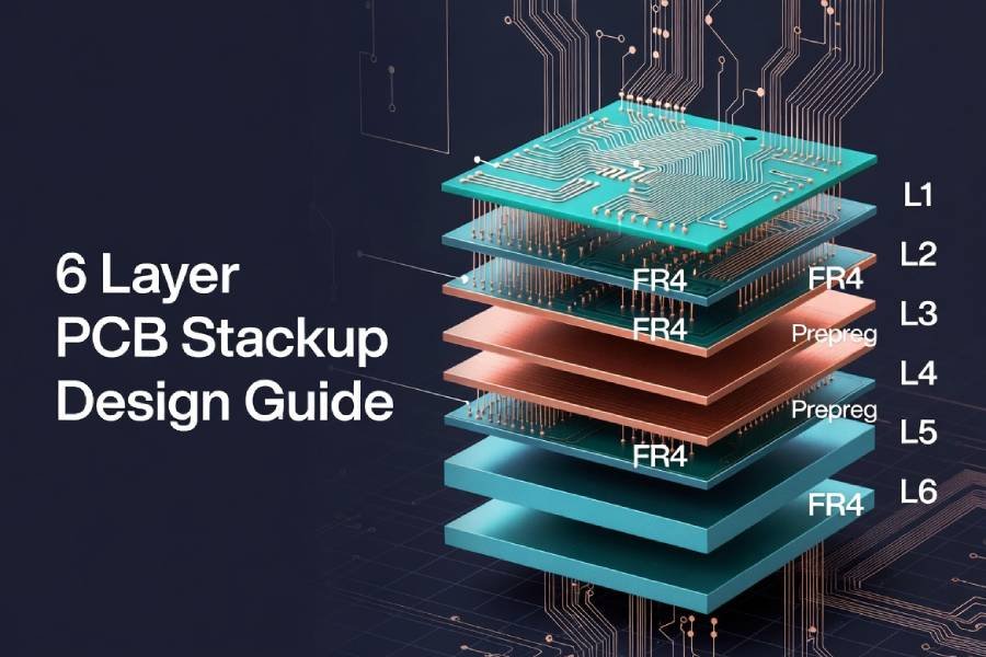
A common starting point for many high‑speed designs is a 4‑layer PCB where the top layer carries most of the high‑speed routes and the second layer is a solid ground plane. A typical functional stackup might look like this (from top to bottom): top signal, ground plane, power and mixed signals, bottom signal and ground.
In this arrangement, controlled impedance traces on the top layer behave as microstrips referenced to the solid ground plane on layer 2, which makes it relatively straightforward to achieve 50 Ω single‑ended and 100 Ω differential impedance using standard FR‑4 materials and realistic trace widths.
For designers, this means that many high‑speed interfaces—such as USB, simple LVDS links or lower‑speed serial buses—can be routed on the top layer with clear return paths and predictable impedance, while the inner layers handle power distribution and less critical signals.
The key is to define the dielectric thickness between layers 1 and 2 and the copper weights up front, so that the line widths calculated for your impedance targets match what your PCB manufacturer can produce consistently.
If you are not sure which 4-layer stackups are most practical for your design, our impedance control PCB fabrication team can suggest standard builds that support common 50 Ω and 100 Ω requirements.
Example 2 – 6‑ or 8‑layer high‑speed board with multiple interfaces
As designs grow more complex and include interfaces such as PCIe, DDR, multi‑lane SerDes and multiple Ethernet ports, a 6‑ or 8‑layer stackup with stripline structures becomes more attractive. One common approach is to dedicate one or two inner layers as high‑speed signal layers sandwiched between solid reference planes, forming symmetric or dual‑stripline structures.
For example, you might use a stackup where layer 3 and layer 4 are both high‑speed signal layers, with ground planes on layers 2 and 5, while the outer layers handle connectors, slower signals and local power.
In this configuration, critical differential pairs for PCIe or high‑speed Ethernet can be routed as striplines between well‑defined ground planes, providing excellent field containment, stable impedance and reduced sensitivity to external noise.
Because the traces are fully embedded in the dielectric, you will typically work with narrower line widths than on microstrip layers, which makes close coordination with your PCB manufacturer on minimum geometry, dielectric thickness options and material choices even more important.
Working with your PCB manufacturer on stackup
Defining a good stackup for controlled impedance is not something you have to do alone. Your PCB manufacturer works with many different stackups every day, across various materials, copper weights and layer counts, and can quickly tell you which combinations are realistic for your budget and lead time.
Treating stackup definition as a collaborative step rather than a one‑way specification usually leads to a more robust and manufacturable controlled‑impedance design.
A practical approach is to share your initial stackup idea and impedance targets as early as possible, even if they are not final. Include your proposed layer order, signal and reference plane assignments, target impedances (for example 50 Ω single‑ended and 100 Ω differential) and any constraints on overall board thickness or materials.
Your manufacturer’s engineering team can then check whether the required dielectric thicknesses and trace geometries fit within standard core and prepreg options, and suggest adjustments where necessary.
In many cases, small changes—such as choosing a slightly different core thickness, adjusting copper weights on certain layers or moving the most critical high‑speed routes to better‑positioned signal layers—can make it much easier to hit your impedance targets with comfortable manufacturing margins.
Agreeing on a detailed stackup and impedance plan before you finalize the layout also reduces the risk that late changes in materials or layer structure will invalidate your simulations or require major rerouting.
Checklist before sending your controlled impedance design for fabrication
Before you release your design for fabrication, it helps to walk through a short checklist to confirm that your stackup and impedance information are complete:
- You have defined target impedance values (for example 50 Ω, 75 Ω, 90 Ω, 100 Ω) and line types (single‑ended, differential, microstrip, stripline) for each controlled‑impedance structure.
- Your stackup drawing shows the full layer order, copper weights and dielectric thicknesses between signal layers and their reference planes.
- The base materials (FR‑4 and/or high‑frequency laminates) are specified, or you have agreed acceptable material options with your PCB manufacturer.
- Your fabrication notes include a clear impedance table that links each target to specific layers and, ideally, to named nets or signal groups.
- You have decided whether you need impedance coupons and TDR testing, and communicated any reporting requirements for critical nets.
If you can check all of these items off, you are in a strong position to get impedance‑controlled boards that behave as expected in the lab and in the field, without excessive back‑and‑forth during fabrication.
Conclusion and next steps
A well‑designed stackup is the foundation of any impedance‑controlled PCB. By understanding how dielectric properties, thicknesses, copper weights and reference planes work together, and by choosing appropriate microstrip or stripline structures, you can give your high‑speed traces a stable environment that supports both signal integrity and manufacturability.
Working closely with a capable PCB manufacturer throughout this process turns your stackup from a theoretical drawing into a repeatable, controlled production process.
If you are planning a new high‑speed or RF design and want support in reviewing your stackup and controlled impedance plan, our engineering team can help you refine your proposal before you commit to fabrication.
To learn more about our capabilities and process, visit our Impedance Control PCB Fabrication service page and share your Gerber files and stackup ideas for a detailed engineering review.