Table of Contents
Why a 4 Layer PCB DFM Checklist Saves You Time and Money
The Real Cost of Skipping DFM
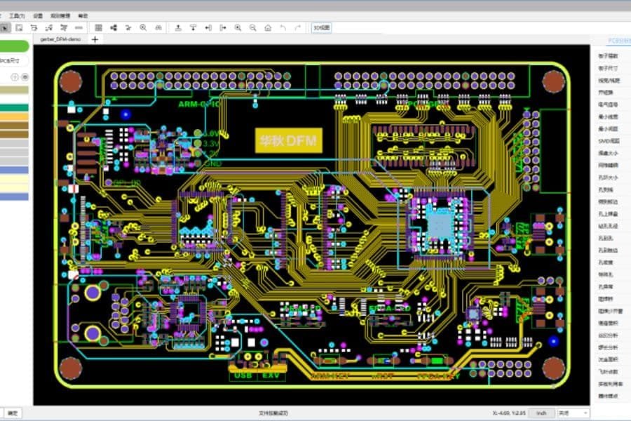
Before you send 4 layer PCB Gerber files to a manufacturer, there is a narrow window where catching mistakes is cheap and easy. Once the board enters the 4 layer PCB manufacturing process—inner layer imaging, lamination, drilling, plating, and E‑test—any DFM issue you missed can mean scrap, engineering holds, or a full respin.
Typical problems like trace/space below capability, via aspect ratios that exceed plating limits, unbalanced copper causing warpage, or incorrect stackup notes do not always show up in your CAD DRC. They show up at the factory, where they translate into added cost, delays, or emails asking you to re‑export files. A clear 4 layer PCB DFM checklist moves these checks upstream so you catch issues while they are still just edits—not scrap.
What This 4 Layer PCB DFM Checklist Covers
This guide focuses specifically on 4 layer PCB DFM guidelines, not generic PCB rules. It covers seven critical areas that directly affect manufacturability and yield:
- Stackup and materials – symmetry, standard thicknesses, copper weight.
- Trace, space, and pads – minimum sizes that align with 4 layer capability.
- Vias and plating – drill sizes, aspect ratios, annular rings.
- Planes and copper balance – warpage control, plane clearances.
- Solder mask, silkscreen, and surface finish – clearances, legibility.
- Panelization and profiling – V‑cut vs tabs, edge clearances.
- Documentation – stackup drawings, fab notes, and test requirements.
Each section includes practical limits plus a checklist item you can mark off before Gerber submission. At the end, you will find a consolidated, printable 4 layer PCB DFM checklist you can turn into an internal standard, along with a link to upload your files for a free DFM review based on these same rules.
Symmetric 4 Layer Stackup and Standard Materials
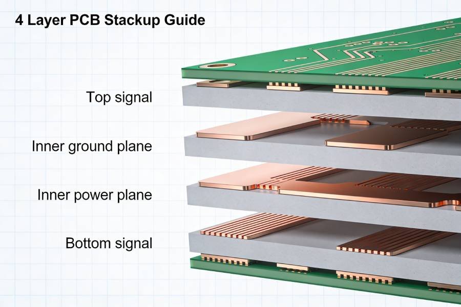
For 4 layer PCB DFM, the stackup is the first place to start, because it drives lamination, warpage, impedance, and cost. A good DFM‑friendly stackup is symmetric, uses standard FR4 materials, and clearly documented in your fabrication notes.
DFM rules for 4 layer PCB stackup and materials:
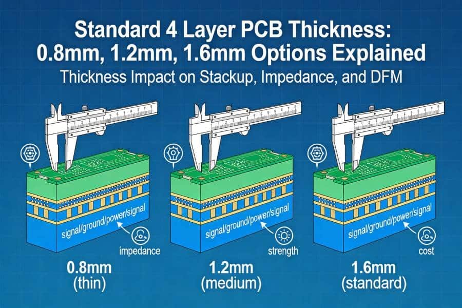
- Use a symmetric 4 layer stackup (e.g., Signal / Ground / Power / Signal or Ground / Signal / Signal / Ground) with mirrored dielectric thickness top and bottom.
- Choose standard FR4 with typical Dk (4.2–4.5) and standard total thickness options (0.8 / 1.0 / 1.2 / 1.6mm) instead of custom thicknesses.
- Keep copper weight realistic: 1 oz on signal layers; 1–2 oz on planes only when needed for current, as heavier copper tightens etch tolerances and raises cost.
Checklist – Stackup & material DFM:
- Stackup is symmetric (dielectric + copper mirrored about center).
- Total thickness is a standard 4 layer value (e.g., 1.6mm).
- Copper weights per layer are specified and realistic (no unnecessary 2 oz everywhere).
- A stackup drawing is included in the fab package (layer names, thicknesses, materials).
Need examples of DFM‑friendly stackups? See your existing 4 Layer PCB Stackup Guide for ready‑to‑use templates.
Trace, Space, and Pad DFM Rules
Minimum Trace Width, Spacing, and Clearance for 4 Layer PCBs
Trace width and spacing are among the most common DFM issues because they directly affect imaging, etching, and inspection capability. For 4 layer PCB DFM, minimums are slightly tighter than 2 layer boards due to the need for reliable plating and inner layer registration, but always stay within your fabricator’s published capabilities.
Standard 4 layer PCB DFM trace/space rules (IPC Class 2, 1oz copper):
- Trace width: ≥6 mil (0.15mm); 5 mil possible (+10–20% cost).
- Trace spacing: ≥6 mil (0.15mm) between traces/pads.
- Pad‑to‑pad: ≥8 mil edge‑to‑edge for SMT.
Power/ground traces: Scale width by current (use calculator); 20+ mil for >1A. High‑speed signals follow 3W rule (spacing = 3x width) to minimize crosstalk.
Checklist – Trace/space/pad DFM:
- All traces ≥6 mil width.
- All spacing ≥6 mil (trace‑to‑trace, trace‑to‑pad).
- SMT pad spacing ≥8 mil edge‑to‑edge.
- No acute angles <45° on traces.
- Power traces sized for current (no <10 mil for >0.5A).
Pad Sizes, Annular Rings, and Solder Joint Reliability
Pads must be large enough for solder joints and registration tolerance. Annular rings (pad around via) are critical for 4 layer boards to survive plating and thermal stress.
Pad DFM rules:
- SMT pads: ≥0.6mm x 0.8mm (0201 min).
- TH pads: Drill +20–30 mil diameter.
- Annular ring: ≥6 mil external/internal.
Checklist – Pad DFM:
- All pads ≥0.6mm for SMT.
- Annular rings ≥6 mil all vias.
- No overlapping pads/traces.
- Thermal reliefs on large planes.
Violations here cause shorts, opens, or weak joints. has full pad libraries.
Vias, Drilling, and Plating DFM Rules
Via Sizing, Aspect Ratio, and Plating Limits for 4 Layer PCBs
Vias are high‑risk for DFM in 4 layer boards because they go through all layers, requiring reliable plating over the full stack height. Poor via design leads to opens, plating voids, or breakout during thermal cycling.
4 layer PCB DFM via rules (standard through vias):
- Drill diameter: ≥8 mil (0.20mm); 6 mil possible (+cost).
- Aspect ratio: ≤8:1 (board thickness / drill dia.); ideally ≤6:1 for 1.6mm boards (e.g., 0.20mm drill max).
- Annular ring: ≥6 mil external, ≥4 mil internal (pad minus drill/2).
No blind/buried vias unless specified—they add sequential lamination and cost. Keep via density reasonable for drill changeovers.
Checklist – Via/plating DFM:
- All via drills ≥8 mil.
- Aspect ratio ≤8:1 (calculate: thickness / smallest drill).
- Annular rings ≥6 mil external / 4 mil internal.
- Vias ≥10 mil from board edge.
- No tenting required unless specified.
Avoiding Common Via Failures
Small drills or high aspect ratios cause plating “dog bones” (voids at ends) or insufficient copper buildup (needs ≥25μm plating). Fanout BGA pins with staggered vias to meet annular ring.
Checklist – Advanced via checks:
- High‑current vias have larger drills (≥12 mil).
- Thermal vias under hot components spaced ≥0.5mm.
- Via in pad only if filled/plugged.
For impedance control, use via calculators from your PCB Tools Guide.
Planes, Copper Balance, and Warpage Prevention
Power/Ground Plane Design and Clearance Rules
Planes provide low‑impedance power delivery but need proper splits, clearances, and stitching to avoid shorts or EMI. In 4 layer PCB DFM, plane splits must not create “slots” under signal traces.
Plane DFM rules:
- Plane clearance: ≥20 mil from splits to traces (anti‑slot rule).
- Split gaps: ≥15 mil wide, with stitching vias ≤λ/20 apart.
- Coupled returns: Keep signals over solid plane sections.
Checklist – Plane DFM:
- Plane splits ≥20 mil from signal traces.
- Stitching vias around splits every 1/4 wavelength.
- No plane under BGA without via fanout.
Copper Balance for Warpage Control
Uneven copper causes warpage during lamination/reflow (up to 0.7% max tolerance). Balance coverage to ±10% across layers using pours or thefting.
Copper balance rules:
- Coverage per layer: 30–70%; mirror high/low density symmetrically.
- Thieving: Add non‑functional copper dots/pours in sparse areas.
- Check tool: Run copper pour analysis in CAD.
Checklist – Copper balance DFM:
- Each layer copper % within ±10% of average.
- Large voids filled with hatched thefting (50% density).
- Warpage spec noted (<0.75%).
Unbalanced planes warp boards—see Warpage Prevention Guide for examples.
Solder Mask, Silkscreen, and Surface Finish DFM
Solder Mask Clearances and Web Requirements
Solder mask prevents solder bridges and protects copper, but poor design causes exposure or weak joints. 4 layer PCB DFM requires precise mask expansion around pads and webs between them.
Solder mask rules:
- Expansion: 4–6 mil (0.1–0.15mm) around pads.
- Web/dam: ≥4 mil between adjacent pads (green mask); ≥5 mil other colors.
- Slivers: No mask <3 mil wide (use gang openings).
Checklist – Solder mask DFM:
- Mask expansion 4–6 mil per side on all pads.
- Minimum web ≥4 mil between pads.
- No thin slivers; gang if <4 mil.
- Vias tented if specified (note HASL/ENIG incompatibility).
Silkscreen Legibility and Clearances
Silkscreen aids assembly—keep it readable and away from solder areas. Minimum height 0.060″ for fab readability.
Silkscreen rules:
- Clearance to pads/mask: ≥5–8 mil.
- Stroke width: ≥6 mil.
- Text size: ≥0.060″ high, 0.008″ stroke.
Checklist – Silkscreen DFM:
- All text ≥0.060″ high, ≥6 mil stroke.
- ≥5 mil from pads/solder mask edges.
- No silkscreen over fiducials/test points.
Surface Finish Selection
Choose based on assembly: HASL for cheap leaded, ENIG for fine pitch. Specify in notes.
| Finish | Use Case | Shelf Life | Cost |
|---|---|---|---|
| HASL | Leaded wave | Short | Low |
| ENIG | Fine pitch, RoHS | Long | Medium |
| OSP | SMT, cheap | Very short | Lowest |
Checklist – Surface finish:
- Finish specified (e.g., ENIG 0.05μm Au).
- Matches assembly (no HASL on <0.5mm pitch).
Silkscreen Template in Design Resources.
Panelization, Profiling, and Edge DFM
V-Cut vs Tab-Routing and Depanelization Rules
Panelization maximizes yield but requires proper spacing, tabs, and fiducials. V-cut suits rectangles; tab-routing (mouse bites) for irregular shapes or edge components.
Panelization rules:
- V-score: Straight edges only, 0mm spacing, components ≥1–2mm from cut.
- Tabs/mouse bites: 2–3mm channels, holes 0.5–0.8mm dia., ≥5mm wide tabs.
- Rails: ≥12.7mm (0.5″) on long sides with tooling holes/fiducials.
| Method | Unit Spacing | Comp-to-Cut | Tab Specs |
|---|---|---|---|
| V-Score | 0mm | ≥1mm | N/A |
| Tabs | 2–3mm | ≥2mm | ≥5mm wide, mouse bites 0.5mm holes |
Checklist – Panelization DFM:
- Panel outline layer included with method specified.
- Components ≥1mm (V)/2mm (tabs) from cuts.
- 3+ fiducials ≥5mm from edges/corners.
- Tooling holes on rails (≥3mm from corners).
Board Edge Profiling and Copper Clearance
Routing tolerances ±0.1mm; keep copper away to avoid shorts/delamination. Slots ≥1mm wide, corners ≥1.5mm radius.
Profiling rules:
- Copper-to-edge: ≥0.5mm (V-cut), ≥0.2mm (routing).
- Castellations/slots: ≥1mm wide, chamfer ends.
Checklist – Profiling DFM:
- Copper ≥0.5mm from all edges.
- Slots ≥1mm, rounded corners.
- Tolerances noted (±0.1–0.15mm typical).
Use Panelization Template from PCBELEC Resources.
4 Layer PCB DFM FAQ
The 4 Layer PCB DFM FAQ addresses the most common questions from design engineers to resolve manufacturing issues quickly.
Recommended: Signal/Ground/Power/Signal or Ground/Signal/Signal/Ground, 1.6mm thick, symmetric to prevent warpage. Place signal layers adjacent to reference planes for impedance control. Use 1oz copper on signals; 2oz on power if needed.
Standard 6/6 mil (0.15mm) for reliability and low cost. 3/3 mil possible at premium fabs (+20–50% cost) for high density. Verify current capacity with calculators.
Aspect ratio = board thickness / drill dia. ≤8:1, ideally ≤6:1. For 1.6mm, use 8 mil (0.20mm) drill min, annular ring ≥6 mil external / 4 mil internal. Avoid microvias to save cost.
Aim 30–70% coverage per layer, ±10% variance; use thieving (hatched pours) in sparse areas. Check with CAD copper analysis tools.
≥4 mil (0.1mm) for green mask, ≥5 mil other colors. Use gang exposure if thinner. Expansion 4–6 mil.
V-cut for rectangles (0mm spacing, components ≥1mm from cut); tab-routing for irregular/edge parts (2–3mm channels, 0.5–0.8mm mouse bite holes). Add 3+ fiducials.
ENIG for fine pitch (<0.5mm)/RoHS (long shelf life); HASL for wave soldering (cheap). Specify thickness e.g., ENIG 0.05μm Au.
Use Gerber viewer for layer alignment; prefer IPC-2581 over RS274X. Required: stackup drawing, impedance table, panel layout, fab notes.
Questions? Upload Gerbers for free DFM check!
Ready to Build Your 4 Layer PCB?
You’ve got the complete 4 layer PCB DFM guide—now put it to work. Download the consolidated checklist, run it on your design, and avoid costly respins. PCBELEC offers free DFM review for your Gerbers: upload today for 99% first-pass yield.
Next steps:
- Export Gerbers + stackup drawing.
- Self-check with this guide.
- – get feedback in 24h.
4 Layer Quick Quote: 1–10pcs from $15/pc, 5–7 day turn.
Complete 4 Layer PCB DFM Checklist (Printable)
Copy to PDF/Excel for printing. Mark off before fab submission.
| Section | Checklist Items |
|---|---|
| 1. Stackup & Materials | [ ] Symmetric stackup (mirrored dielectrics) [ ] Standard thickness (1.6mm) [ ] 1oz signals / realistic plane oz [ ] Stackup drawing included |
| 2. Traces/Space/Pads | [ ] Traces ≥6 mil [ ] Spacing ≥6 mil [ ] SMT pads ≥0.6mm, spacing ≥8 mil [ ] Annular rings ≥6 mil [ ] 45° angles only |
| 3. Vias/Plating | [ ] Drills ≥8 mil [ ] Aspect ≤8:1 [ ] Annular ≥6/4 mil [ ] ≥10 mil to edge |
| 4. Planes/Copper | [ ] Plane splits ≥20 mil from traces [ ] Copper ±10% balance [ ] Thieving in voids [ ] Stitching vias |
| 5. Mask/Silk/Finish | [ ] Mask expansion 4–6 mil [ ] Dams ≥4 mil [ ] Silk ≥0.060″ high, 5 mil clearance [ ] Finish specified |
| 6. Panel/Profiling | [ ] Outline layer w/ method [ ] Comp ≥1–2mm from cuts [ ] 3+ fiducials [ ] Copper ≥0.5mm edge |
| 7. Documentation | [ ] Gerber viewer verified [ ] Fab notes complete [ ] IPC-2581 format |
Total checks: 40+. 100% pass = production ready!