Table of Contents
Why the 4 Layer PCB Manufacturing Process Matters
Who Should Care About the Process
If you are designing or buying a 4 layer PCB, understanding the manufacturing process is not just “nice to have”—it directly influences how you choose your stackup, layer thickness, tolerances, and even your delivery dates. For hardware engineers, knowing how inner layers are imaged, laminated, drilled, and plated helps you set realistic design rules and avoid DFM violations that slow down production or hurt yield. For purchasing and project managers, the process explains why some “simple looking” boards are more expensive or need longer lead times, and what can be done up front to keep cost and risk under control.
A clear picture of the 4 layer PCB manufacturing process also helps align expectations between your design team and your PCB supplier. When everyone understands key steps like lamination, drilling, copper plating, and electrical testing, conversations about stackup changes, thickness options, or delivery estimates become faster and more concrete instead of relying on guesswork.
How Manufacturing Constraints Influence Your Design and Cost
Every major manufacturing step—inner layer imaging, multilayer lamination, via drilling and plating, outer layer etching, solder mask and surface finish, and final electrical testing—comes with its own capabilities and limits. These constraints define what is “easy and economical” versus what needs special handling, extra process steps, or tighter inspection, which all show up in your quote as higher prices or extended lead times.
For example, very thin cores or custom total thicknesses complicate lamination and warpage control, while extremely small vias or very tight trace/space rules push drilling and imaging to their limits. Understanding how your 4 layer PCB travels through the factory allows you to choose stackups, design rules, and finishes that match standard processes, so you get stable quality and predictable delivery without overpaying. In the following sections, we will walk through each step of 4 layer FR4 PCB manufacturing and highlight the DFM considerations you should keep in mind as you design.
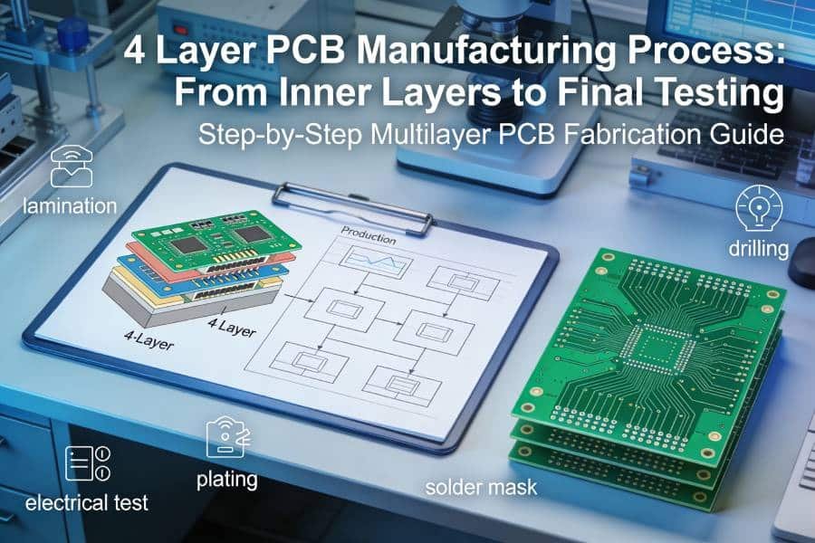
Step 1 – Preparing Materials and Inner Layers
Material Selection: FR4 Core, Copper Thickness, and Standard Stackups
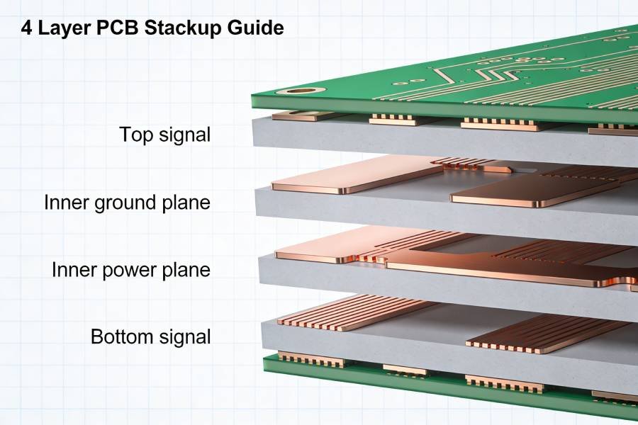
The 4 layer PCB manufacturing process starts with selecting the right FR4 cores, copper thicknesses, and a standard stackup that matches your design and cost targets. A typical 4 layer board uses FR4 glass‑fiber epoxy as the dielectric, with 1 oz copper on each side of the inner core and outer foils, arranged in a Signal / Ground / Power / Signal stackup.
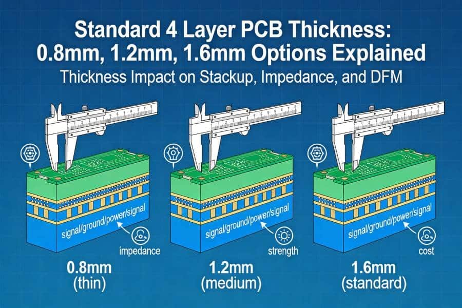
Fabricators usually prepare large copper‑clad laminates that will become the inner layers (Layer 2 and Layer 3) of your 4 layer PCB. These cores are chosen based on your 4 layer PCB thickness (for example 1.6mm vs 1.2mm), target impedance, and standard material sets in the factory. Using one of the manufacturer’s standard 4 layer FR4 stackups helps keep cost and lead time under control.
Inner Layer Cleaning, Photoresist Lamination, Imaging, and Etching
Once the cores are selected, the first active manufacturing step is inner layer imaging and etching, where the copper patterns for the internal planes and traces are created. The copper surfaces are chemically cleaned and micro‑etched to remove oxidation and improve adhesion. The cores are then coated with a dry‑film photoresist, which will protect the areas of copper we want to keep.
Using either film artwork or laser direct imaging (LDI), the desired inner layer circuit pattern is exposed onto the photoresist with UV light. The exposed regions harden, while unexposed regions remain soluble and are washed away during development, leaving bare copper where it should be etched. The panels go through an etching line where chemicals remove the unwanted copper, and finally the hardened photoresist is stripped off, revealing the finished inner layer circuitry—solid ground and power planes, plus any inner signal traces your stackup requires.
Inner Layer Inspection and AOI Before Lamination
Because inner layers will be permanently buried after lamination, quality control at this stage is critical. Each inner layer panel goes through automatic optical inspection (AOI) to check for shorts, opens, line width deviations, and other defects that could cause failure later. The AOI system compares the imaged copper pattern against your Gerber data, flagging any discrepancies for repair or rejection.
Only after passing AOI and visual inspection are the inner layers cleaned again and prepared for lamination. At this point, your 4 layer PCB has well‑defined internal planes and traces, but the outer layers and plated‑through vias do not yet exist. In the next step, these inner cores, prepregs, and outer copper foils are stacked and bonded together to form a single multilayer structure.
Step 2 – Layer Alignment and Lamination
Stack Preparation: Core, Prepreg, and Copper Foils
After the inner layers of your 4 layer PCB have been imaged, etched, and inspected, the next step is to turn them into a single multilayer structure through lamination. For a standard 4 layer FR4 stackup, the manufacturer stacks the etched inner core (Layers 2 and 3) with sheets of prepreg (fiberglass cloth pre‑impregnated with epoxy resin) and outer copper foils that will become Layers 1 and 4.
A typical lay‑up for a standard 4 layer PCB thickness of 1.6mm uses a 0.8mm inner core with 2116 prepreg on both sides and 0.5oz–1oz copper foils on the outside. The exact core and prepreg thicknesses depend on the total thickness and impedance requirements you specified in your 4 layer PCB stackup. Using a factory standard lay‑up minimizes risk and improves yield because the resin content, glass style, and copper weights are already tuned to work well together.
Pinning, Registration, and High‑Temperature Lamination
To ensure that all layers line up correctly, the stacked materials are aligned and pinned using tooling holes or a pin‑lamination system. Good layer‑to‑layer registration is critical: misalignment between inner pads and later drilled holes can cause opens, shorts, or unreliable vias. Once aligned, the stack is loaded into a lamination press that applies carefully controlled heat and pressure.
During lamination, the prepreg resin melts, flows, and cures, bonding the inner core and outer copper foils into a single rigid panel while filling any gaps between layers. Typical lamination cycles for 4 layer PCBs involve temperatures around 170–180°C and pressures in the range of a few hundred PSI, held long enough to fully polymerize the resin. The press then cools down under pressure to avoid introducing internal stresses or voids. This one lamination cycle is usually sufficient for standard 4 layer builds without blind or buried vias.
How Lamination Choices Affect Thickness and Warpage
Lamination parameters and stack symmetry directly influence the final 4 layer PCB thickness and flatness. Uneven resin flow or asymmetric copper distribution between top and bottom layers can lead to bow and twist (warpage), which creates assembly problems and solder joint stress. Balanced stackups—with mirrored dielectric thicknesses and similar copper density on opposing layers—are much more likely to stay within tight warpage limits (often <0.5% of the board diagonal).
From a design perspective, this means choosing standard 4 layer stackups, avoiding large solid copper areas on only one side, and keeping component and plane distribution reasonably symmetrical. If your design is very thin (e.g., 0.8mm) or uses heavy copper, discussing lamination and warpage control with your PCB manufacturer early in the process can prevent surprises later in assembly. After lamination, the result is a flat, bonded 4 layer panel ready for drilling and via formation.
Step 3 – Drilling and Via Formation
Mechanical Drilling for Through‑Holes
Once lamination is complete, the bonded 4 layer panel is ready for drilling, which creates all through‑holes for vias, through‑hole components, and mounting holes. In a standard 4 layer PCB manufacturing process, CNC drilling machines use a drill file derived from your Gerber and drill data to position and drill thousands of holes across the panel with high accuracy.
Hole diameters and locations must respect the factory’s aspect ratio limits—typically around 8:1 to 10:1 (board thickness to finished hole diameter) for reliable plating—so a 1.6mm thick board usually needs finished via sizes of at least 0.2mm–0.25mm. After drilling, the panel edges may be trimmed to remove excess prepreg, and any burrs or rough edges around the holes are removed in a deburring step to prepare for plating.
Desmear and Hole Wall Preparation
Drilling a laminated 4 layer PCB leaves resin smear and glass fibers on the hole walls, which can block electrical contact to the internal copper pads. To fix this, the boards go through a desmear and hole conditioning process: chemical or plasma treatments remove resin smear, lightly etch the hole walls, and expose clean inner‑layer copper pads around each hole.
This preparation step is crucial for good plated‑through hole (PTH) reliability. If smear remains, or if inner pads are not properly exposed, the subsequent copper plating may not adhere consistently, leading to intermittent connections or early failures under thermal stress.
Electroless and Electrolytic Copper Plating to Create PTH Vias
After drilling and desmear, the panel enters the copper metallization stage, where the hole walls and outer surfaces are coated with conductive copper. The process typically begins with electroless copper plating, which deposits a very thin (~0.3–1.0 µm) copper seed layer inside the holes and on the panel surfaces without using electrical current.
This seed layer provides a conductive base for electrolytic copper plating, where the panel is submerged in a copper sulfate bath and connected as a cathode. By passing current through the bath, copper is built up both on the outer layers and along the hole walls, forming robust plated‑through vias that electrically connect all four layers of the PCB. Typical finished hole wall copper thickness for 4 layer PCBs ranges from about 20–25 µm and can be higher for high‑reliability or high‑current designs.
From a design perspective, this means your via sizes, pad diameters, and annular rings must fit both drilling and plating capabilities. Good 4 layer PCB manufacturing DFM ensures via aspect ratios are reasonable, annular rings are wide enough to tolerate registration errors, and there is sufficient clearance between vias and other copper features to avoid shorts during plating.
Step 4 – Outer Layer Imaging and Etching
Dry Film Lamination and Outer Layer Imaging
With plated through‑holes now electrically connecting all four layers of your 4 layer PCB, the next step is to image and etch the outer layers (Layers 1 and 4) to create the final circuit patterns and pad shapes. Unlike inner layers, where photoresist is used as an etch resist, the outer layer process typically involves pattern plating to build up thicker copper where needed for current carrying capacity or reliability.
The process begins with dry film lamination on both sides of the panel, similar to inner layers. The outer layer artwork (from your Gerber files) is aligned and exposed using UV light through film or direct imaging. However, for 4 layer PCBs, the exposure pattern is often reversed compared to inner layers: the areas where you want copper (circuits and pads) remain unexposed and protected, while non‑circuit areas will be etched away.
After development, the panel is ready for selective plating.
Pattern Plating, Etching, and Tin Stripping
Pattern plating deposits additional copper (typically 15–25 µm) and tin (or tin/lead) only on the circuit areas. The panel is connected as a cathode in an electrolytic bath, where current flows preferentially through the exposed copper traces and pads, building thickness for better solderability and current capacity.
The tin plating acts as an etch resist during the final copper etch. Chemicals like sodium hydroxide (NaOH) or ammonium persulfate remove all unprotected copper, leaving only the plated circuit patterns. Finally, the tin is stripped chemically, revealing clean copper ready for surface finish.
This tenting or pattern plating method is standard for 4 layer PCBs because it allows heavier outer copper (1.4–2oz finished) without plating the entire panel, saving time and chemistry costs.
Preparing for Solder Mask and Surface Finish
After outer layer etching, the panel undergoes a thorough cleaning to remove etch residues, ensuring good adhesion for the next steps. At this stage, your 4 layer PCB has all four layers patterned and interconnected by plated vias, but the copper surfaces are still exposed and vulnerable to oxidation. The board is now ready for solder mask application to protect the non‑soldered copper and define pad openings, followed by surface finish to protect the pads themselves for assembly.
Design note: Outer layer tolerances are slightly looser than inner layers since they are visible for inspection, but pad‑to‑trace spacing must still meet your fab house’s DFM rules (typically ≥4–6 mil for Class 2). Misalignment here affects solder joint quality more than inner layer registration.
Step 6 – Profiling, Electrical Testing, and Final Inspection
Routing, V‑Cut, and Panelization
With surface finish applied and silkscreen complete, your 4 layer PCB is ready for profiling to separate individual boards from the production panel. Most 4 layer PCBs are fabricated in panels of 4–18 individual boards (depending on size), held together by tabs, V‑cuts, or mouse bites for efficient processing.
Common depanelization methods:
- V‑Scoring (V‑Cut): Fastest for rectangular boards; angled grooves (45–60°) leave a thin web for clean snap‑separation. Keep components ≥3mm from score lines.
- Tab Routing: Flexible for any shape; breakaway tabs with mouse bites. More handling but better for irregular outlines.
- Tab + V‑Cut Combo: Hybrid for complex panels.
CNC routing mills follow your outline data to cut the board shape, slots, and edge chamfers. V‑cut machines create grooves along straight lines. The choice affects assembly stress—V‑cut is fastest but generates dust; tabs protect edges better.
100% Electrical Test for 4 Layer PCBs
Every finished 4 layer PCB undergoes electrical testing (E‑test) to verify continuity between nets and isolation between non‑connected nets. Flying probe testers make contact with test points and measure opens, shorts, resistance, and capacitance against your netlist—critical for multilayer boards where internal defects are invisible.
E‑test checks:
- Opens/Shorts: 100% netlist verification.
- Resistance: Low ohms for power nets, high megohms isolation.
- Capacitance: Confirms layer integrity (plane shorts).
For high‑reliability, Kelvin 4‑wire testing measures true resistance without probe contact error. Yield <99.5% triggers investigation; failures are repaired or scrapped.
Final Visual Inspection, Packaging, and Shipping
Final inspection combines AOI for surface defects (solder mask voids, missing silkscreen) with manual visual checks for scratches, contamination, and dimensional accuracy. Fiducials, legends, and edge quality are verified against your drawings.
Cleaned and vacuum‑bagged boards are packaged in moisture‑barrier bags with desiccant for ESD and humidity protection. Shipping documents include test reports, stackup drawings, and material certifications. Your 4 layer PCB is now production‑ready.
How 4 Layer PCB Manufacturing Differs from 2 Layer Boards
Extra Process Steps and Cost Drivers
While 2 layer PCBs are made by directly imaging and etching copper‑clad laminates, 4 layer PCB manufacturing involves significantly more steps to create and interconnect the buried inner layers. The inner layer imaging, etching, and inspection alone add 2–3 days and 30–50% to the cost compared to double‑sided boards.
Key differences:
- 2 Layer: Single panel imaging → etch → drill/plate → outer finish (4–5 steps).
- 4 Layer: Inner layers → lamination → drill/plate → outer layers → finish (8–10 steps).
Lamination and the need for precise inner layer registration drive most of the added complexity and cost. Designers moving from 2 to 4 layers should expect longer lead times and higher per‑board prices, but gain vastly improved EMI performance, routing density, and signal integrity.
What Designers Should Keep in Mind When Moving from 2 to 4 Layers
4 layer PCB manufacturing DFM is stricter than 2 layer because inner defects are invisible and plating must connect four copper layers reliably. Key considerations:
- Aspect ratio: 4 layer boards are thicker, so minimum via size increases (e.g., 0.25mm finished for 1.6mm board).
- Plane splits: More stitching vias needed around splits to ensure plating continuity.
- Copper balance: Symmetric distribution prevents lamination warpage.
Checklist for 2→4 layer designers:
- Verify stackup against fab capabilities (standard vs custom).
- Increase annular rings 10–20% for registration tolerance.
- Add fiducials and test points for E‑test.
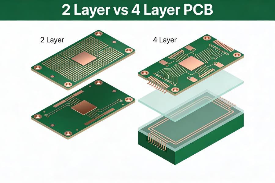
Read our 2 Layer vs 4 Layer PCB guide for full comparison, including manufacturing impacts.
Design Tips to Make 4 Layer PCB Manufacturing Smoother
DFM Rules That Align with the Manufacturing Process
Understanding the 4 layer PCB manufacturing process lets you design for it, reducing cost, lead time, and respins. Here are 4 layer PCB manufacturing DFM guidelines tied to each major step:
Inner Layer Imaging/Etching:
- Trace/space ≥6/6 mil (5/5 possible, +10–20% cost).
- No acute angles (<45°); use arcs for smooth etching.
- Minimize solid copper areas (>80% density causes under‑etch).
Lamination:
- Copper balance ±10% between symmetric layers (prevents warpage).
- Use standard stackups; custom dielectrics +15–25% cost.
- Fiducials ≥3mm from edges for registration.
Drilling/Plating:
- Aspect ratio ≤10:1 (1.6mm board → ≥0.16mm drill).
- Annular ring ≥6 mil all vias/pads.
- Via antipad ≥8 mil larger than drill.
Outer Etching/Solder Mask:
- Mask clearance ≥4 mil; ≥0.1mm preferred.
- Pad‑to‑trace ≥6 mil for HASL.
- Thermal pads with solder paste openings.
What to Include in Your Fabrication Notes and Stackup Drawing
Complete fab package accelerates 4 layer PCB fabrication:
Stackup Drawing:
Layer 1 (Top Signal): 1.4oz
Prepreg 2116: 0.11mm (H=0.12mm)
Layer 2 (GND): 1oz
Core 0.8mm
Layer 3 (PWR): 1oz
Prepreg 2116: 0.11mm
Layer 4 (Bottom): 1.4oz
Total: 1.60mm ±0.10mm
Fab Notes:
- “100% E‑test required. HASL surface finish. V‑scoring on X axis. Green LPI solder mask.”
- “Min trace/space 6/6 mil. Aspect ratio 10:1 max.”
Checklist Before Gerber Submission:
- Stackup drawing matches Gerbers
- Drill file units correct (metric/imperial)
- Panelization specified (tabs/V‑cut)
- Test points ≥4 per net
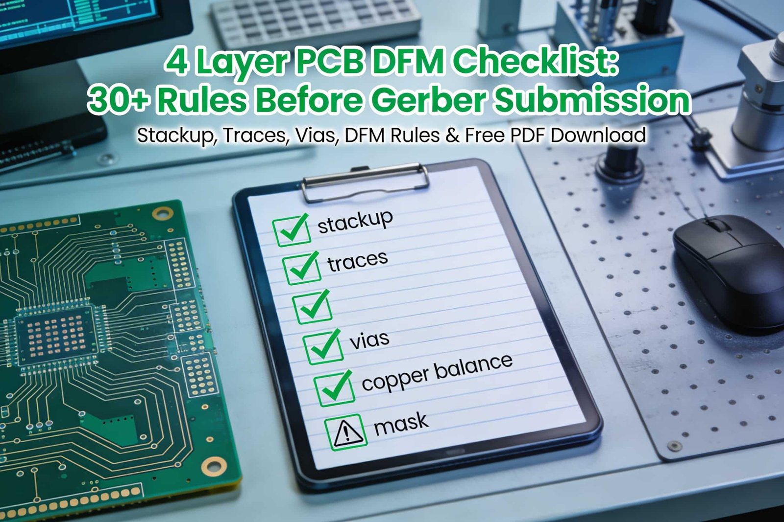
Download 4 Layer PCB DFM Checklist for full template.
FAQ: Common Questions About 4 Layer PCB Manufacturing
Standard 4 layer PCB manufacturing process for prototypes (1.6mm, standard features) typically takes 3–5 working days after Gerber approval, plus 1–2 days for DFM review if needed. Production volumes extend shipping but not fab time.
4 layer adds inner layer imaging/etching and lamination, doubling process steps and cost while enabling buried planes for EMI/signal integrity. Drilling/plating connects 4 layers vs 2. See our 2 vs 4 Layer guide.
After mechanical drilling and desmear (removing resin smear), electroless copper seeds holes, followed by electrolytic plating to build ~25µm copper walls connecting all layers.
Asymmetric copper distribution, uneven prepreg flow, or mismatched thermal expansion. Fix with ±10% copper balance and standard symmetric stackups. 4 Layer PCB Stackup Guide covers this.
Yes, flying probe or bed‑of‑nails E‑test verifies opens/shorts on every net before shipping. Multi‑layer boards get extra capacitance checks for plane integrity.
HASL (cost‑effective, good shelf life), ENIG (flat, lead‑free, RF), OSP (eco‑friendly). Choice affects assembly and cost—specify in fab notes.
Follow 4 layer PCB manufacturing DFM: 6/6 mil trace/space, standard stackup, stitching vias at splits, copper balance, ≥10mm edge clearance. 4 Layer DFM Checklist has full rules.
Ready to Build Your 4 Layer PCB? Let's Make Manufacturing Smooth
You now have the complete roadmap of the 4 layer PCB manufacturing process—from inner layer etching and lamination to drilling, plating, outer imaging, surface finish, and final E‑test. Understanding these steps helps you design smarter, avoid costly DFM issues, and collaborate better with your fabricator for reliable, on‑time production.
Further reading in our 4 Layer PCB series:
- 4 Layer PCB Stackup Guide – Stackup planning
- Standard 4 Layer PCB Thickness – Thickness selection
- 4 Layer PCB Design Guidelines – Layout rules
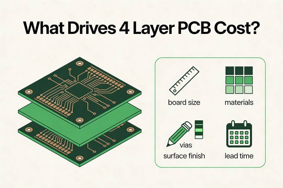
- What Drives 4 Layer PCB Cost? – Pricing factors
- 2 vs 4 Layer & 4 vs 6 Layer – Layer decisions
Ready to manufacture your 4 layer PCB? Upload Gerbers for free DFM review + process validation + firm quote. Our team checks stackup, registration risks, plating feasibility, and tolerances against our 4 layer PCB manufacturing process capabilities, ensuring first‑pass success.