Table of Contents
Most real products today are neither “pure SMT” nor “pure through-hole”—they are mixed-technology boards where fine‑pitch BGAs and tiny passives sit alongside big connectors, transformers, and other leaded parts that still make sense as THT.
When you add RoHS and lead-free requirements on top, combining SMT reflow with through-hole soldering on a single PCB stops being a simple routing problem and becomes a process-integration challenge.
Lead-free reflow runs hotter and tighter than legacy SnPb, while lead-free wave and selective soldering have their own constraints around pallets, masking, and thermal loading on previously reflowed SMT joints.
Layout choices, hole design, and process sequence all influence whether your mixed assembly runs smoothly or is plagued by solder shorts, insufficient fill, overheated components, and extra rework.
This article is written for designers, process engineers, and manufacturing teams who are building mixed-technology PCBs with lead-free SMT and through-hole on the same board.
We will look at typical process flows, key design rules, thermal and fixturing tactics, and common defect modes, so you can plan mixed assemblies that are not only manufacturable in a lead-free world but also reliable and predictable in volume production. To add internal links from this new mixed-technology article to your service pages, we can follow the same pattern as before: insert a few contextual, descriptive anchor texts at natural points in the copy.
Why Use Mixed Technology with Lead-Free Processes?
What “Mixed Technology” Means in Modern PCBs
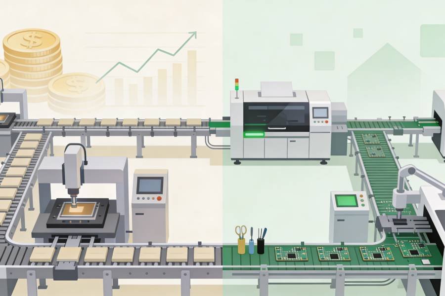
Mixed-technology PCB assembly simply means building boards that use both surface-mount technology (SMT) and through-hole technology (THT) on the same PCB.
SMT parts sit directly on the board surface and are soldered in a reflow oven, enabling dense layouts, high-speed signals, and efficient automated placement, while through-hole parts sit in drilled vias and are soldered from the opposite side, offering strong mechanical anchoring and robustness for heavy or stressed components.
This combination lets designers use small, fast SMT packages where space and performance matter, and reserve through-hole footprints for connectors, large capacitors, transformers, and other parts that see mechanical load, heat, or frequent plugging and unplugging.
The result is a board that can be compact and feature-rich without sacrificing robustness where it really counts—especially in industrial, automotive, power, and control applications.
Typical Use Cases for Combining Lead-Free SMT and Through-Hole
In a RoHS and lead-free context, mixed technology is often the default rather than the exception: most small and medium components are only available as lead-free SMT, while many high‑current connectors or legacy parts remain through-hole.
Typical examples include power supplies with SMT controllers and THT magnetics, control boards with dense SMT logic plus rugged THT I/O connectors, or industrial modules where relays and large capacitors share space with compact SMT signal chains.
Using lead-free SMT and THT processes together on one board does add complexity, because hotter lead-free profiles and multiple soldering steps must be coordinated so that earlier joints and components are not damaged by later operations.
When that integration is planned from the design stage—rather than left as a detail for the factory to “figure out”—mixed-technology, lead-free assemblies can deliver high reliability and manufacturability without excessive rework or cost.
Process Flow: Lead-Free SMT Reflow, Wave, and Selective Soldering
Standard Build Sequence on a Mixed Lead-Free Board
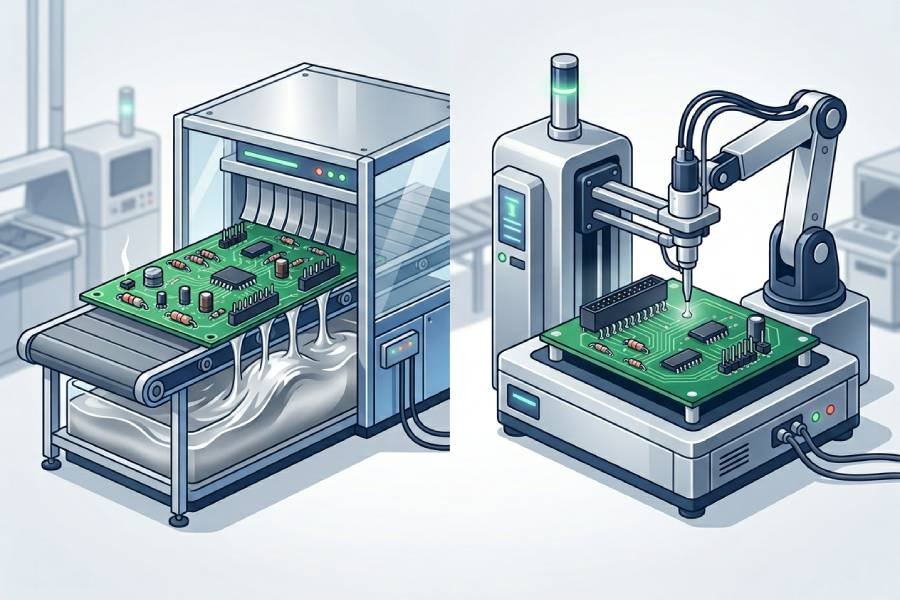
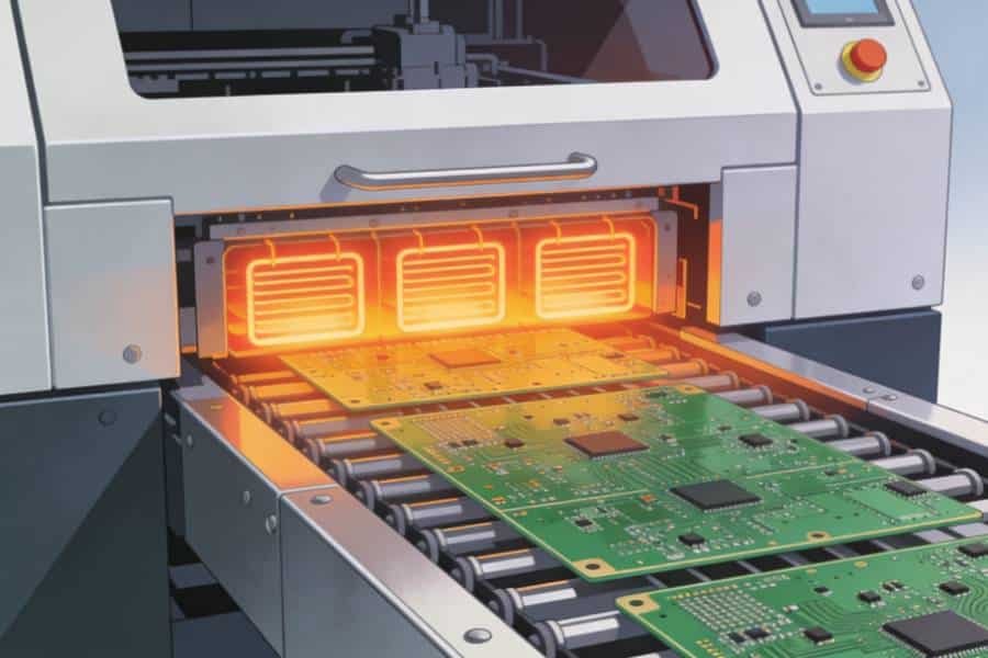
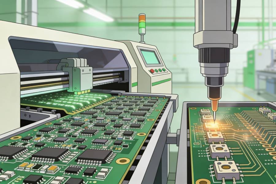
On most mixed-technology, lead-free boards, the standard sequence is to solder SMT components first with reflow, then handle through-hole parts using wave or selective soldering.
This approach protects delicate SMT packages from direct contact with a solder wave and ensures that the hottest, most profile‑sensitive step (lead-free reflow) happens before any additional heating from THT processes.
A typical flow looks like this: print lead-free solder paste, place SMT, run the board through a lead-free reflow profile, inspect, then insert through-hole components and solder them using wave, selective soldering, or intrusive reflow where appropriate.
Hand soldering is often reserved for truly exceptional cases, such as very low volumes, special components, or rework where automated methods are impractical.
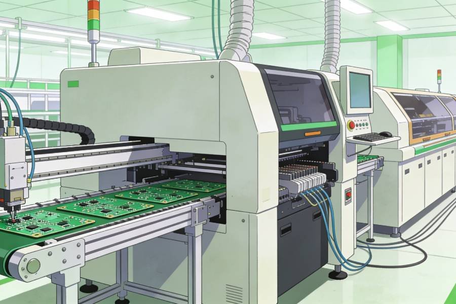
Lead-Free Wave Soldering in a Mixed SMT/THT Context
In classic mixed-technology wave soldering, the already‑reflowed SMT components—typically on the top side or selectively on the bottom—are protected using pallets or carriers while the board passes over a lead-free solder wave to solder the exposed through-hole leads.
These pallets are custom machined from heat‑resistant composites and act as both mechanical support and a mask that shields bottom‑side SMT pads and components from molten solder.
The wave process itself usually includes fluxing, preheat, and then one or more waves (turbulent followed by laminar) tuned for lead-free alloys, with careful control of conveyor speed and immersion depth.
When set up well, wave soldering can produce hundreds of consistent THT joints in a single pass, but dense layouts and fine‑pitch THT can increase the risk of bridging or insufficient fill if pallet design and process parameters are not optimized.
When to Use Selective Soldering Instead of Wave
Selective soldering is often the better choice for dense mixed-technology boards, especially when you have tight SMT placement near through-hole pads or only a small number of THT joints per board.
Instead of immersing the entire underside in a solder wave, selective soldering uses programmable nozzles or mini‑waves to apply flux and solder only where needed, dramatically reducing thermal stress on nearby SMT components.
Selective soldering trades some throughput for precision: it is slower than a full wave on high‑pin‑count THT, but it reduces masking effort, lowers rework rates, and provides more consistent joint quality on complex boards.
For many lead-free mixed assemblies—especially with double‑sided SMT, tight clearance, or high‑value boards—the combination of reflow plus selective soldering has become the mainstream hybrid process flow.
Design Guidelines for Mixed Lead-Free SMT and Through-Hole
Component Placement and Keep-Out Strategies
Good mixed-technology layouts start with clear zoning: group SMT components where reflow makes sense and reserve dedicated areas for through-hole parts that will see wave or selective soldering.
Designers often keep most SMT on one side (typically the top) and cluster THT components—connectors, power parts, large mechanical items—in regions where pallets or selective nozzles can access them without running into dense SMT.
You should also respect keep-out distances between THT pins and nearby SMT pads, especially anywhere a wave might pass; guidelines commonly call for at least 0.5–2 mm clearance depending on process and pallet design.
Clear silk markings for polarities and orientations, plus consistent component orientation in the direction of the wave, help reduce assembly errors and improve solder drainage.
Pad, Hole, and Thermal Relief Design for Lead-Free THT
Lead-free THT joints must contend with higher soldering temperatures and often slightly different flow behavior than SnPb, so pad and hole design become more critical.
Holes should provide reasonable annular ring and a lead-to-hole ratio that allows proper capillary action—too tight and you risk insufficient fill, too loose and solder control becomes harder, especially with lead-free alloys.
When THT pins connect to large copper planes or power nets, thermal relief pads are usually recommended so the barrel can heat evenly without drawing excessive heat into the plane during wave or selective soldering.
Well‑designed thermal reliefs balance electrical performance with manufacturability, reducing the need to push processes to hotter or longer profiles just to get acceptable barrel fill on a few “stubborn” pins.
Managing Shadowing, Solder Thieving, and Double-Sided SMT
Mixed-technology layouts are especially vulnerable to wave soldering issues like shadowing, where tall components block solder flow to pins behind them, and bridging, where solder accumulates between closely spaced leads.
You can mitigate these risks by aligning rows of pins in the wave direction, staggering tall components to minimize “shadows,” and using solder thieves at the ends of dense pin rows to pull excess solder away from functional pads.
If you have SMT on both sides, pay special attention to which side sees reflow first and how the second‑side process (wave or selective) will interact with bottom‑side parts.
In many designs, it is safer to keep bottom‑side SMT small and well away from THT pads that will be wave‑soldered, or to plan on selective soldering instead of wave where clearances are tight.
Thermal, Fixturing, and Profile Considerations
Coordinating Lead-Free Reflow and THT Heating
On a mixed-technology board, SMT components may experience two significant heat exposures: first during lead-free reflow, then again during wave or selective soldering of through-hole parts.
Because lead-free alloys run at higher temperatures than SnPb, you need to ensure that the combined thermal budget of these steps stays within component and laminate ratings, especially for plastics, adhesives, and moisture‑sensitive devices.
This coordination starts with choosing reflow profiles and THT soldering parameters (preheat, solder temperature, dwell time) that are “just hot enough” for reliable joints, then checking that the most heat‑sensitive components and PCB materials can tolerate the worst‑case combination of both processes.
For critical assemblies, simulating or measuring top‑side temperatures during wave/selective soldering and validating with test coupons or early builds helps avoid latent damage such as delamination or package cracking.
Pallets, Carriers, and Masking for Mixed Assemblies
Custom wave solder pallets and selective solder fixtures are central tools for controlling both solder contact and thermal exposure in mixed-technology lead-free assemblies.
These pallets are machined from heat‑resistant composite materials to hold the PCB rigid, expose only the desired through-hole leads, and shield bottom‑side SMT components, gold fingers, and other sensitive features from direct solder contact.
Integrated masking in the pallet design can eliminate much of the manual masking with tape or peelable solder mask, reducing labor and the risk of residue or missed spots.
Well‑designed pallets also improve process repeatability by controlling immersion depth, stabilizing board flatness over the wave, and minimizing defects like bridging and solder mask damage.
Dealing with Large Connectors and High Thermal-Mass Parts
High pin‑count connectors, thick boards, and large thermal‑mass components are often the most challenging parts to solder reliably in a lead-free mixed process.
Their mass can keep barrels cooler than surrounding areas, leading to incomplete hole fill unless preheat, solder temperature, and dwell time are carefully tuned—and even then, the risk of excessive copper dissolution or component body overheating increases as you push the process.
Design tactics such as providing sufficient annular ring, appropriate thermal reliefs, and good access for selective nozzles or local heating tools make robust joints easier to achieve.
In some high‑reliability or very high thermal‑mass cases, specialized rework or soldering equipment (for example, local vapor phase or dedicated THT rework systems) may be justified to meet barrel‑fill and reliability requirements without overstressing the rest of the assembly.
Lead-Free Process and Reliability Challenges in Mixed Assemblies
Common Defects: Shorts, Insufficient Fill, and Skips
Lead-free mixed-technology assemblies tend to see the same broad categories of defects as traditional builds—shorts, opens, insufficient solder, and voids—but hotter profiles and tighter process windows can make some of these more frequent if the process is not well tuned.
In wave and selective soldering of through-hole joints, typical lead-free problems include insufficient hole fill, solder bridges between adjacent pins, and solder skips where a pin receives little or no solder due to shadowing or poor wetting.
These issues often trace back to a combination of factors: marginal lead-to-hole ratios, inadequate flux coverage, suboptimal preheat or dwell times, or board layouts that make it hard for solder to flow uniformly around the pins.
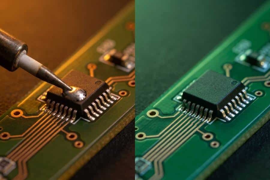
On the SMT side of the same board, classic lead-free defects like voiding, tombstoning, and cold joints can also appear if reflow profiles and paste volumes are not tuned for the actual thermal distribution of a mixed assembly.
Lead-Free Alloy Behavior in Through-Hole Joints
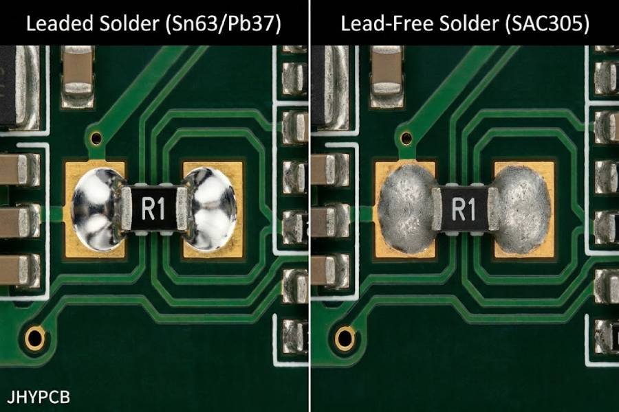
Lead-free alloys such as SAC305 wet differently and are generally less ductile than SnPb, which affects how THT joints behave under mechanical and thermal stress.
They tend to form stiffer joints with different intermetallic growth patterns in the barrel and at the pad interface, which can be either a benefit or a risk depending on how thick those intermetallic layers become during soldering and aging.
Higher soldering temperatures and longer time above liquidus in lead-free wave and selective soldering can promote thicker intermetallics and more copper dissolution if the process is pushed too hard, especially on high‑thermal‑mass connectors.
From a reliability standpoint, that makes it important to balance wetting and hole fill against excessive thermal exposure, and to consider enhanced lead-free alloys or doped SAC variants where long‑term mechanical stability is critical.
Inspection and Test Strategies for Mixed Technology Boards
Because mixed assemblies combine hidden SMT joints, exposed THT barrels, and sometimes high pin counts, inspection and test strategies need to cover all these joint types without driving cost through the roof.
AOI is typically used to check SMT placement and fillets, while THT joints are inspected visually or with endoscopic tools for barrel fill, solder meniscus shape, and signs of skips or bridging.
X‑ray inspection can be valuable for verifying hidden SMT joints and confirming through-hole fill on critical connectors, especially when lead-free processes and tight layouts make visual access difficult.
Electrical tests such as ICT and functional test then provide a final safety net, catching opens, shorts, and marginal joints that slipped past visual and X‑ray inspection, and helping you correlate particular defect patterns back to specific parts of the mixed lead-free process for further optimization.
Practical Tips for Working with Your Assembly Partner
Communicating Mixed-Technology Requirements Upfront
Mixed-technology success starts with how you document and communicate requirements to your EMS provider, not just with the Gerbers you send.
Your fabrication and assembly drawings should clearly indicate which components are SMT vs through-hole, preferred wave direction, areas that must be masked, any no‑wave zones, and whether specific THT joints are intended for wave, selective soldering, or hand solder.
Including notes on lead-free alloys, required barrel fill criteria for critical connectors, and any components with tight thermal limits helps your EMS choose suitable profiles, pallets, and fixtures from the start.
The more your documentation reflects real process constraints, the less often your EMS will need to “guess” or ask for late clarifications that can delay builds.
Communicating mixed-technology requirements clearly in your fabrication and assembly drawings helps your EMS choose the right combination of reflow, wave, and selective soldering steps—and if you are still looking for a partner, our lead-free SMT and through-hole PCB assembly services are designed specifically for these mixed boards.
Cost and Lead-Time Drivers in Mixed Lead-Free Assemblies
Compared with pure SMT boards, mixed-technology assemblies introduce extra cost and lead-time drivers that are worth understanding.
Custom wave pallets or selective solder fixtures add non‑recurring engineering (NRE) cost and a bit of extra lead time, but they can reduce unit cost over volume by cutting down on hand masking, rework, and scrap.
Selective soldering programs themselves need to be developed and verified, which shows up as process engineering time, especially on the first few builds.
High‑mix, low‑volume projects may see more of that cost in engineering and setup, while stable, higher‑volume products usually amortize it, making mixed lead-free assemblies cost‑effective once the process is dialed in.
Questions to Ask About Lead-Free Mixed-Technology Experience
When you evaluate or brief an assembly partner for lead-free mixed-technology work, targeted questions can quickly reveal their level of experience.
Useful questions include how often they build lead-free mixed SMT/THT boards, whether they design and maintain their own pallets and fixtures, and what their typical defect rates are for lead-free wave/selective soldering (shorts, insufficient fill, skips).
You can also ask for examples of similar boards they have built, how they handle thermal profiling when SMT sees multiple heating steps, and what inspection and test strategies they use for complex mixed assemblies.
Partners who can show you sample fixtures, process documentation, and defect/repair metrics for lead-free mixed-technology jobs are far more likely to deliver consistently reliable results than those speaking only in generalities.
Conclusion
Mixed-technology PCB assembly lets you combine the density and efficiency of lead-free SMT with the mechanical robustness of through-hole, but it also ties your design success directly to how well reflow, wave, and selective soldering are integrated on the same board.
Layout choices, pad and hole design, thermal management, fixturing, and process tuning all interact in a lead-free environment; if any one of those pieces is treated as an afterthought, the result is often shorts, insufficient fill, excessive rework, or compromised reliability.
The good news is that with clear zoning of SMT and THT areas, sensible pad and thermal relief design, carefully designed pallets or selective solder fixtures, and inspection and test strategies tailored to mixed assemblies, lead-free mixed-technology boards can run reliably at scale.
The most effective teams treat their EMS provider as a process partner—sharing intent, constraints, and reliability targets up front—so mixed-technology, lead-free assembly becomes a predictable, repeatable part of the product lifecycle rather than a recurring source of surprises on the factory floor.