Gold Finger PCB DFM Checklist: 10 Things to Check Before Sending Gerbers
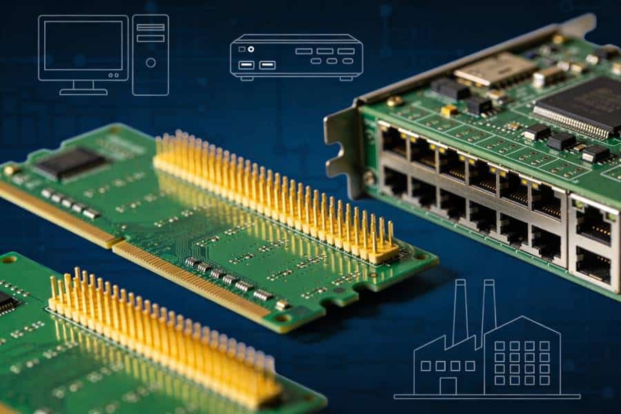
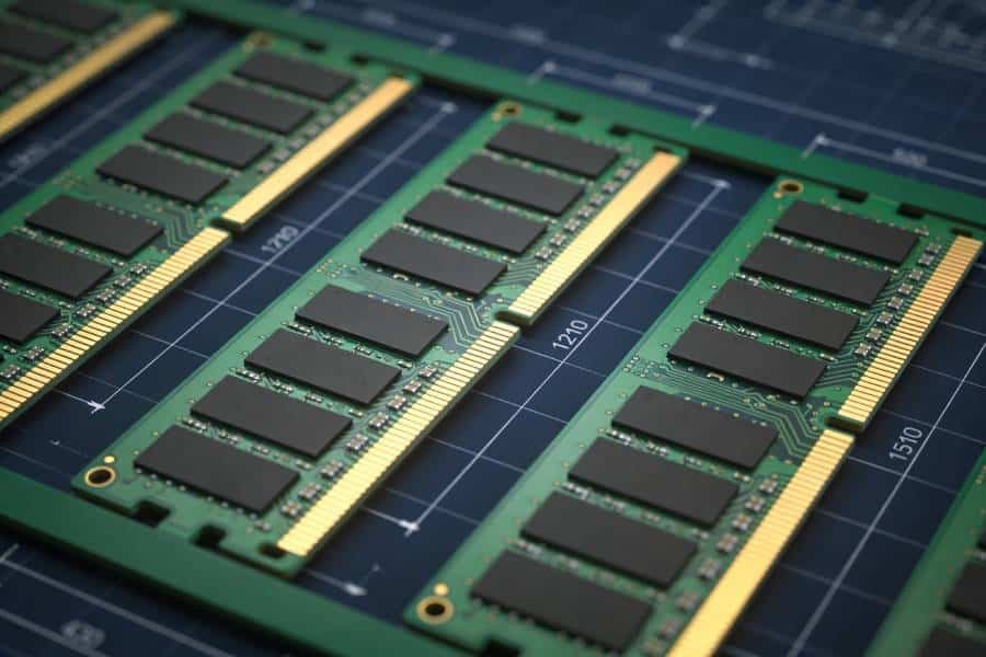
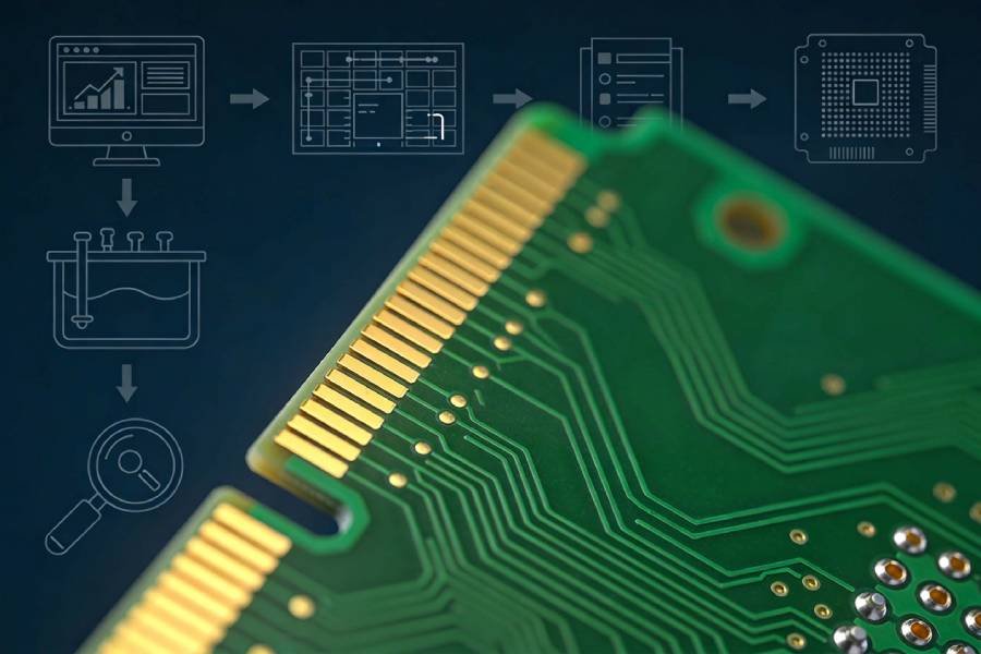
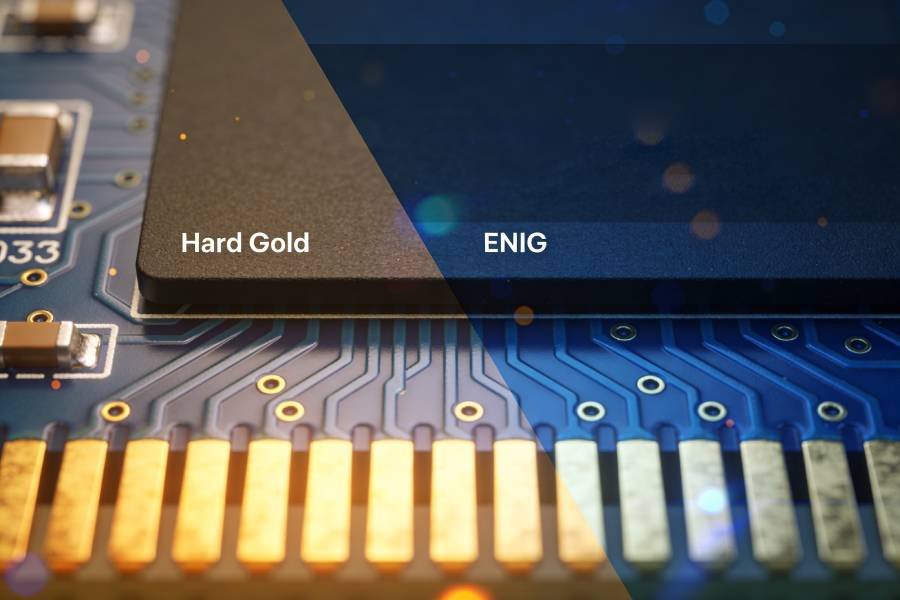
Gold finger PCBs fail in the field more often because of DFM oversights than connector theory. This checklist walks you through 10 things to verify before sending Gerber files, from finger geometry, bevel and finish definitions to copper clearances, keep-outs, and panelization. Use it as a last pre-flight check to catch issues early and make your manufacturer’s DFM review much smoother.
Gold Finger PCB DFM Checklist: 10 Things to Check Before Sending Gerbers Read More »