BGA Assembly: Selection, Design & Reliability
A practical guide for engineers choosing BGA packages — when to select BGA over QFP/LGA, key PCB design challenges, and common reliability failure modes.
Why Choose BGA: Package Selection Advantages
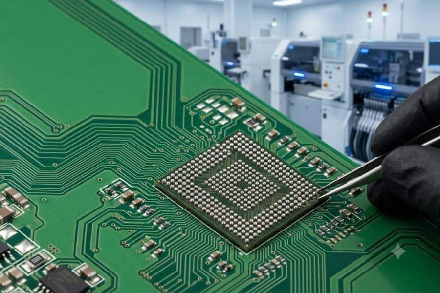
Ball Grid Array (BGA) packages are preferred over perimeter-leaded packages like QFP when a design requires high pin counts, superior thermal dissipation, or high-speed signal integrity. BGA’s grid-array connection provides more I/O in less board area while maintaining shorter electrical paths.

- 1. Higher I/O Density — BGA uses the full underside area for connections, supporting 3,000+ pins in a single package. QFP is limited to perimeter leads, capping practical pin count at approximately 240.
- 2. Superior Thermal Performance — Solder balls create a direct thermal path from die to PCB. Many BGA packages include thermal pads or heat spreaders, dissipating heat more effectively than QFP leads.
- 3. Better Electrical Characteristics — Shorter interconnect paths reduce parasitic inductance and capacitance, improving signal integrity for high-speed applications such as DDR memory, PCIe, and SerDes links.
- 4. Self-Alignment During Reflow — Surface tension of molten solder balls pulls BGA components into correct alignment during reflow. This self-centering effect improves placement tolerance and first-pass yield compared to QFP.
BGA is the right choice when your design needs more than 200 I/O pins, high-speed signal integrity, or significant thermal dissipation. For simpler designs under 100 pins, QFP or SOIC may be more cost-effective.
BGA Design and Layout Challenges
Designing PCBs for BGA components requires careful attention to fanout routing, via structures, and pad geometry. Fine-pitch BGAs (0.4–0.5mm) often demand HDI construction with blind and buried vias, while larger BGAs need controlled warpage to prevent solder joint defects during reflow.
| Challenge | Description | Design Impact |
|---|---|---|
| Fanout & Escape Routing | Traces route from BGA pads to outer layers via breakout patterns. Fine-pitch BGAs may need 1–2 via channels per ball row. | Determines layer count and board cost |
| Via-in-Pad Plated (VIPPO) | Vias placed directly under BGA pads, then filled and plated flat. Essential for pitch ≤0.5mm where space prevents dog-bone fanout. | Prevents solder wicking; adds fabrication cost |
| Board Warpage Control | Reflow temperatures (240–260°C) can warp PCBs, causing opens at BGA edges. Use high-Tg materials (Tg≥170°C) and symmetric copper distribution. | Prevents head-in-pillow and open joints |
| Pad Design (NSMD vs SMD) | NSMD (Non-Solder Mask Defined) exposes full copper pad — preferred for BGA. SMD confines solder within mask openings. NSMD offers better wetting and stress distribution. | Affects joint reliability and crack resistance |
| Solder Mask Webbing | Solder mask between adjacent BGA pads must be ≥50μm wide to prevent mask leg lifting and solder bridging. Fine-pitch BGAs challenge this limit. | Prevents bridging; impacts assembly yield |
Submit your BGA land pattern and stackup for DFM review before fabrication. Incorrect pad geometry or via placement is the leading cause of BGA assembly failures.
BGA Reliability — Understanding Failure Modes
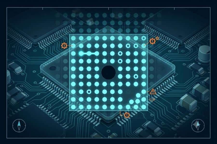
BGA solder joints are hidden beneath the package, making defect detection difficult without X-ray inspection. Understanding common failure modes and their root causes helps designers and manufacturers implement preventive measures that ensure long-term joint reliability.
- 1. Head-in-Pillow (HIP) — The solder ball and paste deposit touch during reflow but fail to coalesce into a single joint. Caused by package warpage, excessive paste volume, or inadequate soak time. Requires angled X-ray (45–70°) to detect.
- 2. Cold Joints / Non-Wet Opens — Solder ball and paste fail to bond due to insufficient reflow temperature, oxidation, or contamination. Results in intermittent or open connections that may pass initial testing but fail in the field.
- 3. Excessive Voiding — Gas pockets trapped in solder joints, measured as percentage of pad area. IPC-A-610 allows ≤25% (Class 2) and ≤10% (Class 3). Excessive voids reduce mechanical strength and thermal conductivity.
- 4. Thermal Cycling Fatigue — Repeated temperature cycling causes differential expansion between BGA substrate, solder joints, and PCB, leading to crack propagation and eventual joint fracture. Mitigated by CTE matching and compliant underfill.

Specify IPC-A-610 Class 3 inspection for safety-critical BGA applications. Require 100% X-ray inspection, void measurement reports, and thermal cycling test data from your assembly partner.
Need Professional BGA Assembly?
JHYPCB provides BGA assembly with 100% X-ray inspection, 0.4mm fine-pitch capability, and expert rework services. ISO 9001 & IATF 16949 certified.
Frequently Asked Questions About BGA Assembly
BGA is preferred when a design requires more than 200 I/O pins, high-speed signal integrity, or significant thermal dissipation. QFP is limited to perimeter leads (typically under 240 pins), while BGA uses the full package area, supporting 3,000+ connections. For designs under 100 pins, QFP or SOIC is often more cost-effective.
Via-in-pad places routing vias directly under BGA solder pads, then fills and plates them flat. VIPPO is required for fine-pitch BGAs (0.5mm or less) where there is no space for traditional dog-bone fanout routing. It prevents solder wicking into the via, which would starve the BGA joint of solder. VIPPO increases PCB fabrication cost but is essential for HDI BGA designs.
Head-in-pillow is a BGA solder defect where the solder ball and paste deposit touch during reflow but fail to coalesce into a single joint. It is caused by package warpage during reflow, excessive solder paste, or insufficient soak time. HIP defects are difficult to detect — they require angled X-ray inspection (45–70 degrees) and may cause intermittent field failures.
Thermal cycling causes differential expansion between the BGA substrate, solder joints, and PCB, creating cyclic stress that leads to crack propagation and eventual joint fracture. The coefficient of thermal expansion (CTE) mismatch between package and board accelerates fatigue. Underfill, CTE-matched materials, and SAC305 solder with controlled reflow profiles help mitigate thermal cycling damage.
ENIG (Electroless Nickel Immersion Gold) is the most recommended surface finish for BGA assembly. Its flat, coplanar surface ensures uniform solder ball contact, and the nickel layer provides a diffusion barrier that maintains joint integrity during reflow. OSP and lead-free HASL are acceptable for standard-pitch BGAs (0.8mm or more), but ENIG is preferred for fine-pitch (0.5mm or less).
Voiding is minimized by using an optimized reflow profile with adequate soak time (60–120 seconds above liquidus), nitrogen atmosphere for lead-free SAC305 solder, appropriate solder paste with low-volatile flux, and correct stencil aperture design. IPC-A-610 allows 25% or less voiding (Class 2) and 10% or less (Class 3). 100% X-ray inspection verifies compliance.

Ready to Start Your BGA Project?
JHYPCB provides professional BGA assembly services with 100% X-ray inspection, fine-pitch capability down to 0.4mm, and expert rework support. ISO 9001 & IATF 16949 certified.
Prefer email? Send your Gerber files and BOM directly to sales@pcbjhy.com.
Engineering review available for prototype, low-volume, and production BGA assembly projects.