
Table of Contents
Introduction
BGA and QFN are both widely used IC packages in modern PCB assembly, but they serve different design priorities. If a project demands high pin density, compact routing, or advanced processing capability, BGA often becomes the stronger fit; if the focus is on smaller footprints, simpler assembly, and practical thermal performance, QFN may be the better option.
The challenge is that package selection is never just about the component itself. In real PCB assembly, it is also necessary to think about inspection, rework, thermal behavior, and manufacturing risk, especially because both BGA and QFN can hide critical solder joints beneath the package body.
This guide compares BGA and QFN from a PCB assembly perspective, so readers can choose the package that aligns with board density, production process, and reliability goals. This direct, structured approach also aligns with Google’s guidance to publish clear, useful, non-commodity content for readers rather than generic summary content.
What BGA Is
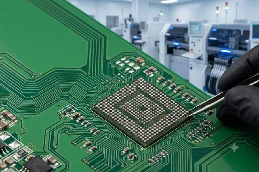
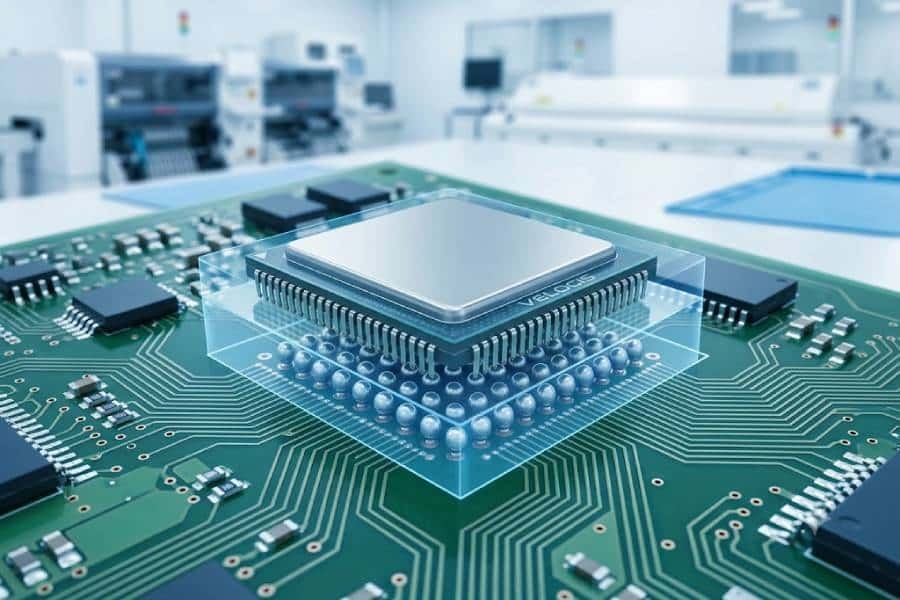
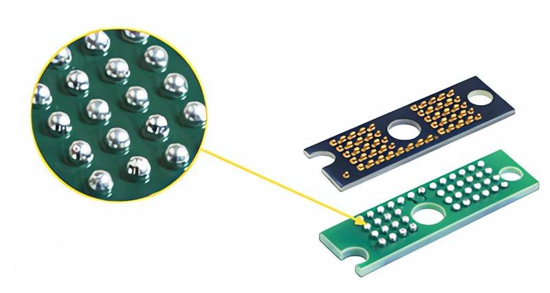
BGA, or Ball Grid Array, is a surface-mount IC package that uses a grid of solder balls on the underside of the component to connect it to the PCB. This structure is widely used for complex chips because it supports high interconnect density and efficient board-level routing.
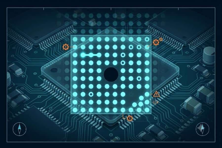
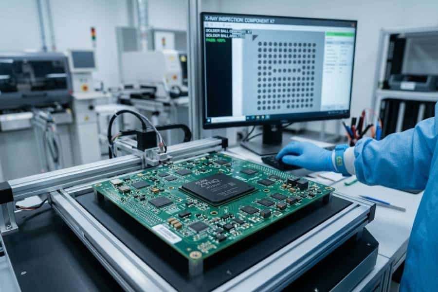
In PCB assembly, BGA is typically mounted through reflow soldering onto corresponding pads on the board. Because the solder joints sit underneath the package body, they cannot be fully checked with simple visual inspection, which is why BGA assemblies commonly rely on X-ray inspection for quality verification.
What QFN Is
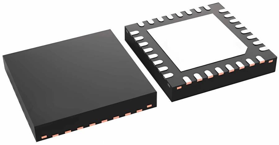
QFN, or Quad Flat No-Lead, is a leadless package that connects through bottom pads and usually includes a central exposed pad for thermal transfer. Compared with BGA, QFN is often used in compact designs where small footprint, practical thermal performance, and manageable assembly complexity are important.
From a PCB assembly standpoint, QFN is attractive because it is usually simpler to place and route than a high-pin-count BGA, but it still presents inspection challenges because key solder joints are located under the package body. That means production teams still need careful process control, and in many cases X-ray inspection remains useful for validating solder quality.
BGA vs QFN at a Glance
BGA is generally the better choice when higher pin density, denser routing, and stronger support for complex ICs are required. QFN is often the better fit when the goal is a smaller package, practical thermal performance, and a simpler assembly profile.
Both packages are leadless and both can hide solder joints under the body, so inspection is not optional in many serious builds. In real PCB assembly, BGA usually requires more complex inspection and rework handling, while QFN is often easier to manage but still benefits from X-ray in critical products.
| Factor | BGA | QFN |
|---|---|---|
| Pin density | Higher, better for complex ICs | Lower, suitable for moderate pin counts |
| Board space | Efficient for dense routing and high functionality | Compact and practical for smaller designs |
| Thermal performance | Strong for high-performance devices, depending on package and board design | Strong thermal path through the exposed pad |
| Inspection | Usually requires X-ray because joints are hidden | Often also benefits from X-ray for hidden-pad defects |
| Rework | More difficult and riskier | Easier than BGA, though still process-sensitive |
| Assembly cost | Typically higher due to process complexity | Often lower and simpler to assemble |
Pin Count and Routing
BGA is usually preferred when the chip has a large number of I/O connections and the PCB needs efficient fan-out routing. Because the solder balls are arranged in a grid, BGA can support denser interconnects than many other packages, which makes it a natural fit for processors, advanced chipsets, and other high-complexity devices..
QFN is often used when the design needs a smaller footprint but does not require the same level of connection density. It can still support solid electrical performance, but once the pin count climbs, BGA often becomes the more scalable choice for layout and routing.
Thermal Performance
QFN often stands out because of its exposed pad, which creates an efficient thermal path from the package to the PCB. That makes it especially useful in compact designs where heat dissipation matters but the device does not require extremely high pin counts.
BGA can also offer strong thermal behavior, especially in high-performance components, but its thermal performance depends heavily on the package design and board-level implementation. In practice, thermal selection is less about which package is universally better and more about how well the package works with the specific power and layout requirements of the device.
Inspection and Rework
This is one of the most practical differences for manufacturers. BGA solder joints sit underneath the package body, so visual inspection cannot fully verify solder quality, and X-ray inspection is commonly used to check for hidden issues such as voids, opens, and other solder-joint defects.
QFN is somewhat easier to handle than BGA in many builds, but it still has hidden solder areas under the body, especially around the central pad. That means critical assemblies may still need X-ray validation, and rework still requires careful process control even if the package is less demanding than BGA.
Manufacturing Cost
Cost is where package choice starts to affect the entire production flow, not just the BOM. In PCB assembly, BGA usually pushes up manufacturing cost because it requires tighter process control, more complex inspection, and more difficult rework handling, while QFN is often simpler and cheaper to assemble.
The more useful way to think about cost is total assembly cost rather than component price alone. Placement complexity, X-ray inspection, yield loss, test strategy, and repair effort all influence the final cost of building the board.
BGA assemblies usually require more advanced inspection and more careful process validation because the solder joints are hidden beneath the package body. For high-density or high-performance designs, that extra cost is often justified by the routing and electrical benefits that BGA makes possible.
QFN often fits lower- to mid-complexity products better because it is usually easier to place, inspect, and assemble than BGA. If the product can meet its electrical and thermal requirements with QFN, the simpler assembly profile may reduce cost without compromising reliability.
Manufacturer’s Perspective
From a PCB assembly manufacturer’s point of view, the choice between BGA and QFN is not just about package size or pin count. It is also about whether the production line can place, inspect, test, and rework the part with the level of control the design requires.
BGA usually demands more process discipline because the solder joints are hidden and the rework process is more specialized. That means the manufacturer must rely on stronger process control, X-ray inspection, and careful reflow management to keep yield and reliability under control.
QFN is often easier to assemble than BGA, but it still needs proper pad design, thermal control, and inspection planning. In other words, QFN may reduce manufacturing complexity, but it does not eliminate manufacturing risk.
Which Package Fits Best
The easiest way to choose is to match the package to the product’s real constraints. BGA is usually the better choice for high pin count, dense routing, and advanced ICs, while QFN is often the better fit for compact products that still need good thermal performance and a simpler assembly flow.
If the board is already tight on space and the chip needs many connections, BGA often solves the layout problem more cleanly. If the design needs a small footprint but does not require extreme I/O density, QFN usually gives a more practical balance of size, cost, and manufacturability.
Use BGA When
- The design has a large number of I/O connections or uses a high-performance processor.
- Dense routing or fan-out makes lower-density packages hard to use effectively.
- The manufacturing plan includes X-ray inspection and stronger rework capability
Use QFN When
- The product needs a compact package with manageable assembly complexity.
- The exposed pad offers a practical thermal path for the application.
- The design can meet its performance target without the added cost and process burden of BGA
Conclusion
BGA and QFN are both excellent package options, but they solve different problems. BGA is usually the stronger choice for high pin count, dense routing, and advanced ICs, while QFN is often the better fit for compact designs, practical thermal performance, and simpler manufacturing.
In PCB assembly, the best choice is not the package with the most technical advantages on paper. It is the package that fits the board layout, inspection strategy, rework capability, and overall production budget most effectively.
If the design is pushing the limits of pin density or system complexity, BGA can provide the headroom required. If the priority is a smaller footprint with a more manageable assembly flow, QFN may deliver the better balance of performance and cost.
For teams evaluating package options for the next PCB assembly project, the best starting point is a design and manufacturing review that considers performance, reliability, and assembly risk together.