
Table of Contents
Why DFM Matters for Low Cost PCB Assembly
Design for Manufacturability, or DFM, matters because the cheapest PCB assembly decision is often made before fabrication begins—at the stage where stack-up, layout, package selection, board outline, and testability are still flexible.
In practical manufacturing, DFM is the process of aligning a PCB design with the real capabilities and cost windows of the factory, so the board can be built with fewer special steps, less rework, and a lower risk of delay or scrap.

For low cost PCB assembly, this matters even more because cost reduction is rarely achieved by one dramatic change. Instead, it usually comes from removing layers of avoidable complexity: too many layers, overly fine design rules, difficult component placement, unnecessary through-hole parts, awkward board outlines, or test access that was never considered until the end.
Each of these choices may look small during design, but together they can increase tooling effort, assembly time, inspection difficulty, and the likelihood of engineering questions or process exceptions during production.
A strong DFM approach also helps prevent one of the most expensive problems in electronics manufacturing: discovering manufacturability issues after the design is already committed to procurement or build preparation.
When that happens, the result is often redesign, BOM revision, panel changes, delayed quotes, or even scrapped boards—all of which cost far more than making the right adjustments early.
This is why DFM should not be treated as a final checklist performed after layout is complete. In cost-sensitive PCB assembly, DFM works best when it shapes decisions from the beginning, guiding engineers toward standard materials, manufacturable trace and spacing rules, practical package choices, panel-friendly outlines, and assembly methods that fit the intended production stage.
Seen this way, DFM is not just a manufacturing review step. It is one of the clearest ways to design specifically for low cost PCB assembly while still protecting yield, reliability, and quoting efficiency.
Aligning PCB Stack-Up and Layer Count with Cost
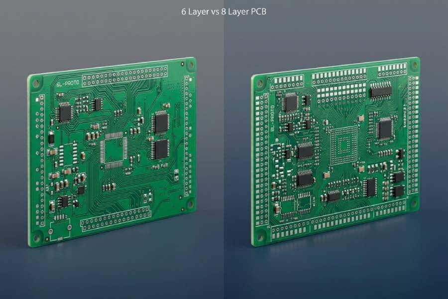
Stack-up and layer count decisions set a large part of the baseline cost for any PCB, and they directly influence how economical the eventual PCB assembly can be.
Every additional layer adds material, additional processes in fabrication, and tighter constraints on routing and drilling, which together increase the per‑board price and often tighten process windows for soldering and test.
Optimize Layer Count for Cost Efficiency
From a DFM perspective, a common recommendation is to use the lowest layer count that still cleanly meets electrical and layout requirements, rather than defaulting to a higher count “just in case.”
Industry DFM rules often highlight that going from 2 to 4 layers, or from 4 to 6, does not simply double cost but can significantly increase both fabrication complexity and yield risk, especially when stack‑ups involve multiple plane layers, fine geometries, or non‑standard materials.
For low cost PCB assembly, this means spending time early to see whether careful routing, better use of planes, and disciplined placement can keep a design at 2 or 4 layers instead of 4 or 6, especially for prototypes and low‑volume builds where each board carries a larger share of fixed tooling and setup costs.
When a higher layer count is genuinely required—because of signal integrity, shielding, or dense routing—a DFM‑aware stack‑up still aims to use structures that are familiar to the factory, avoiding exotic combinations that demand special lamination cycles or non‑standard prepregs.
Use Standard Materials and Thickness Where Possible
Material choices and board thickness also have a strong influence on manufacturing cost. Many DFM guides suggest starting with standard FR‑4 and common thicknesses such as 1.6 mm, which align with default setups for a wide range of PCB manufacturers.
Standard materials and thicknesses tend to fit into well‑understood drill, plating, and press cycles, making it easier for fabricators to maintain yield and for assemblers to rely on predictable warpage and mechanical stiffness during soldering.
By contrast, special materials (high‑Tg, RF substrates, hybrid stack‑ups) or non‑standard thicknesses often require separate production panels, different lamination profiles, and additional process verification, all of which add cost and extend lead time.
For low cost PCB assembly, the practical takeaway is to reserve special materials and thicknesses for designs that truly need them, and to design the majority of cost‑sensitive boards to live comfortably within the “sweet spot” of the manufacturer’s standard stack‑up library.
When stack‑up and layer count are aligned with these standard, cost‑efficient windows, both fabrication and assembly become easier to quote and more forgiving to build—helping low cost PCB assembly remain low cost without requiring the assembler to fight the physics of an over‑complex board.
Via and Routing Strategies for Low Cost Assembly
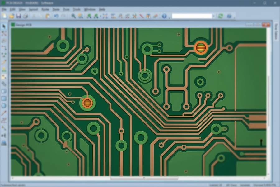
Via strategy and routing rules have a direct impact on both fabrication and assembly cost, because they determine drilling complexity, plating cycles, solderability, and how easily automated equipment can place and solder components.
A DFM approach for low cost PCB assembly focuses on keeping via structures as simple as possible, using manufacturable trace widths and clearances, and avoiding via practices that require special processes unless they are genuinely justified.
Choose Cost-Appropriate Via Types
From a cost perspective, plated through-hole (PTH) vias are still the most economical and robust option for most designs.
Blind, buried, and microvias enable very high routing density and compact form factors, but they demand additional lamination steps, tighter fabrication controls, and often incur explicit “HDI” surcharges, especially at low and mid volumes.
DFM guidelines for cost-sensitive PCBs therefore recommend minimizing the number of via types used in a design and reserving blind or buried vias for cases where there is no practical alternative—such as very dense BGAs or strict stack height constraints.
Standardizing on a single via drill size where possible, and limiting the total number of distinct drills, also simplifies tooling and reduces drill time, which contributes to lower base board cost before assembly even begins.
Keep Vias out of Pads Unless Necessary
Via‑in‑pad technology, where vias are placed directly inside component pads, is sometimes unavoidable for high‑density BGAs or RF components, but it requires special handling such as via filling and planarization to prevent solder wicking during reflow.
These extra processes increase fabrication cost and can complicate assembly if not executed perfectly, because poorly treated via‑in‑pad structures can starve solder joints or trap voids.
For low cost PCB assembly, the general DFM recommendation is to avoid via‑in‑pad wherever feasible, instead using short fan‑out traces and placing vias just outside pads so that standard PTH processes can be used without extra filling or capping steps.
When via‑in‑pad is truly necessary, it should be limited to the components that demand it and clearly documented in fabrication notes, so that both the fabricator and assembler can plan for the added process complexity and cost.
Use Manufacturable Trace Widths and Spacing
Routing with unnecessarily fine trace widths and spacings is another common way to push a design into more expensive process categories.
DFM rules from many manufacturers emphasize designing to their standard capability window—for example, trace/space at or above their “preferred” values rather than always pushing toward the minimum advertised limits.
Staying within those standard rules provides more process margin, improves yield, and reduces the likelihood that a design will require special handling or additional design iterations.
For low cost PCB assembly, this translates into fewer defects to catch at AOI or test, less rework, and more predictable soldering behaviour, all of which support the goal of reducing total assembly cost without sacrificing reliability.
Together, these via and routing strategies—cost‑appropriate via selection, careful control of via‑in‑pad usage, and manufacturable trace/space choices—help ensure that the PCB can be fabricated and assembled using standard, well‑understood processes, which is exactly where low cost PCB assembly works best.
Component Selection and Placement for Low Cost Assembly
Component selection and placement decisions strongly influence how easily and cheaply a PCB can be assembled, reworked, and inspected.
DFM for low cost PCB assembly therefore focuses on standardizing packages, limiting unique parts, simplifying placement, and keeping enough clearance for automated assembly and practical inspection.
Standardize Package Families and Reduce Unique Parts
Every new package type or unique component adds overhead: different feeder setup, different pick‑and‑place parameters, extra verification, and sometimes different soldering behaviour.
Industry DFM and cost‑reduction guides consistently recommend standardizing on a small set of package families—for example, using 0603/0805 passives instead of mixing many different sizes—and reducing the total number of distinct part numbers where possible.
Fewer unique components mean simpler kitting, shorter setup times, and more efficient SMT programming, which is especially important in low‑volume or high‑mix builds where each setup cost is amortized over fewer boards.
From a low cost PCB assembly standpoint, selecting widely available, multi‑sourced components in common packages is one of the most effective ways to keep both material and assembly costs under control.
Place SMT Parts on One Side Where Possible
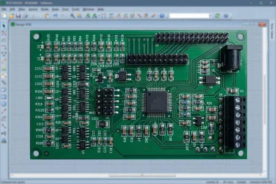
Placing SMT components on both sides of a PCB usually requires at least two reflow cycles and more complex handling, which increases assembly time and the risk of defects.
DFM best practices therefore advise designers to keep as many components as possible on a single side, especially for prototypes and low‑volume runs where each extra process step carries a proportionally higher cost.
Single‑sided SMT layouts allow one efficient reflow profile, simpler fixturing, and fewer concerns about parts dropping or tombstoning during second‑side processing.
When two‑sided assembly is unavoidable, concentrating heavier and more thermally demanding components on one side and lighter components on the other helps maintain stability and reduces rework during low cost PCB assembly.
Respect Clearances for Assembly, Rework, and Inspection
Even with good component choices and side assignments, poor placement can drive up cost if it makes assembly, inspection, or rework difficult.
DFM guidelines emphasize maintaining adequate spacing between components so that solder paste can be printed cleanly, placement heads have room to operate, and tools such as soldering irons or hot‑air nozzles can reach specific pads without disturbing neighbouring parts.
Similarly, leaving room for AOI cameras and ensuring silkscreen markings are clear and not buried under components make inspection faster and more reliable.
For low cost PCB assembly, this means treating spacing, orientation, and labelling not just as aesthetic or convenience features, but as cost drivers: well‑spaced, consistently oriented components are easier to place, easier to test, and easier to fix if something goes wrong.
Panelization and Board Outline Choices
Panelization and board outline choices determine how efficiently boards can be grouped, handled, and separated in production, which has a direct effect on both fabrication and assembly cost.
For low cost PCB assembly, the goal is to design boards that fit well into standard panel sizes, use simple outlines, and include the necessary panel features so that each pass through printing, placement, and soldering handles multiple boards with minimal waste and rework.
Design for Standard Panel Sizes and Simple Outlines
Panelization reduces per‑unit cost by spreading setup and process time across multiple boards in a single panel.
Guides on panelization stress that arranging boards to maximize panel utilization—sometimes improving material usage by 10–25%—is one of the most effective ways to lower both bare PCB and assembly cost.
To achieve this, designers are encouraged to use rectangular or otherwise panel‑friendly outlines, especially for smaller boards that will otherwise need rails or complex break‑off structures.
Standard panel sizes (for example, 18 × 24 inches and similar dimensions) and clear minimum/maximum board sizes are documented by many manufacturers; aligning board dimensions with those preferred ranges helps the factory nest boards efficiently and avoid custom panel setups.
For low cost PCB assembly, this means treating board outline and size as cost levers: simplifying shapes, aligning with standard panel dimensions, and avoiding arbitrary cut‑outs or protrusions where possible.
The simpler and more regular the board, the more likely it is that panelization will reduce per‑board handling and contribute directly to lower assembly cost.
Include Fiducials and Panel Features Early
Beyond size and shape, panelized boards need fiducials, tooling holes, and appropriate edge clearances to support accurate placement and safe depanelization.
Assembly DFM rules typically call for global fiducials on the panel, local fiducials on fine‑pitch component areas, and sufficient clearance between components and board edges so that scoring, routing, or other depanelization methods do not damage solder joints.
Standard recommendations include keeping at least a few millimetres of “keep‑out” zone at panel edges and around mouse‑bites or V‑groove lines, and adding rails when boards are very small or have overhanging components.
These panel features make it easier for pick‑and‑place, AOI, and test equipment to handle the panel as a stable unit, which is especially important when pursuing low cost PCB assembly—any instability or damage at depanelization quickly turns into scrap or rework cost.
By designing with panelization and outline constraints in mind from the start, rather than treating them as a post‑layout detail, designers give manufacturers more room to use standard, efficient panel strategies that reduce both fabrication and assembly costs.
Designing for Testability in Low Cost PCB Assembly
Design for Testability (DFT) ensures that assembled boards can be verified efficiently, so defects are caught early without resorting to slow, manual probing or expensive late‑stage debugging.
In cost‑sensitive projects, DFT is a key part of low cost PCB assembly because well‑planned test access allows shorter test times, simpler fixtures, and fewer surprises, which together reduce overall manufacturing cost and risk.
Add Accessible Test Points and Clear Labelling
Effective DFT starts with deciding which nets and functional blocks need direct access, then adding test points, pads, or dedicated headers to support those checks.
Guidelines from test and manufacturing specialists recommend placing clearly defined test points for power rails, key signals, and interfaces, and designating them in the schematic as non‑BOM components so they appear consistently in layout and documentation.
For fixture‑based testing, it is typically easier and more economical when test points are on a single side of the board, with adequate size and spacing.
Practical layouts often target test point diameters around 0.8–1.3 mm and center‑to‑center spacing near 2.54 mm where space allows, while keeping test points back from board edges and away from tall components on the probe side so fixtures can seal and probes can contact reliably.
Clear silkscreen labels for test points, including reference designators and net names, further reduce setup and debug time, especially in prototypes and low‑volume runs where technicians rely heavily on visual cues.
Match Test Strategy to Volume and Risk
Different projects justify different levels of test, and aligning testability with volume and risk is essential for low cost PCB assembly.
For early prototypes and internal tools, designers might prioritize a modest number of test points and simple functional tests, relying more on visual inspection and manual probing to control cost.
As designs move toward low‑volume production—especially when boards ship to customers or support safety‑relevant functions—DFT often expands to support flying‑probe or ICT coverage, requiring more systematic test point placement and consistent spacing.
In high‑reliability or safety‑critical applications, DFT may include comprehensive access to critical nets, boundary‑scan structures, and dedicated connectors for in‑system testing, reflecting the higher cost of failure in the field.
For all these cases, DFT decisions made during layout effectively set the ceiling for test coverage; retrofitting test points later is usually more expensive than choosing them deliberately at design time.
From a low cost PCB assembly perspective, this means using DFT to avoid both extremes: under‑testing that leads to field failures and over‑testing that adds unnecessary fixture and test time cost.
Working with Your CM on DFM Feedback
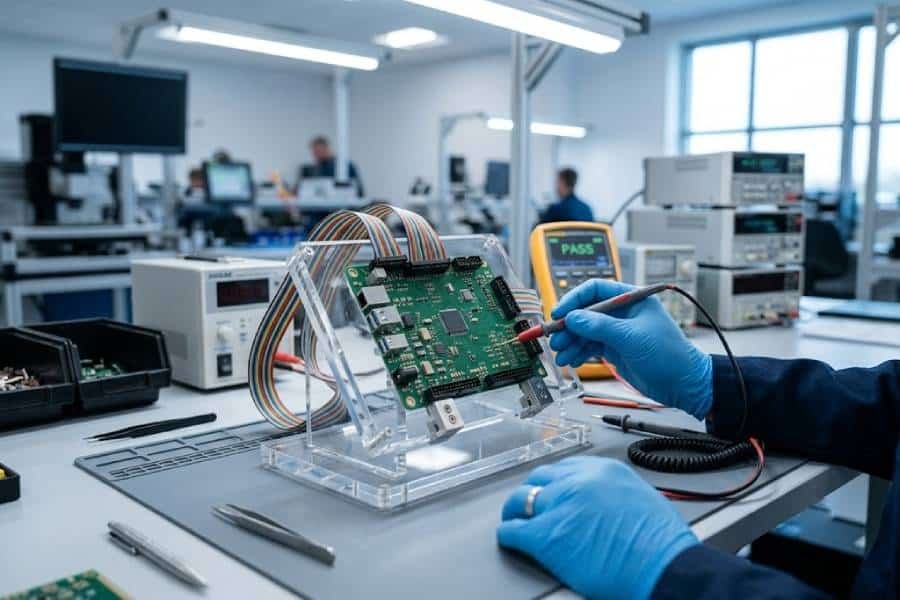
Even a well‑designed board benefits from early and structured feedback from the contract manufacturer (CM) who will actually build it.
DFM reviews performed by the CM help identify features that are hard to fabricate or assemble, predict potential defects, and suggest more cost‑effective alternatives that still meet design intent—often before any material is ordered.
Share Designs Early and Ask for DFM Review
Many manufacturers now offer formal DFM review services, where they run your design through a checklist and automated checks to flag problems such as inadequate clearances, non‑standard drill or pad sizes, risky footprints, or panelization issues.
Best practice is to provide your CM with preliminary design packages early—including stack‑up assumptions, preliminary BOM, and intended volumes—so they can comment on high‑impact cost drivers like layer count, via structures, materials, and panel strategies before the design is frozen.
This kind of early collaboration is particularly valuable for low cost PCB assembly because it allows CMs to point out where a design is forcing them into non‑standard processes or unnecessary risk, and to propose simpler options that fit their standard capability window.
Even when designers have followed their own internal DFM checklist thoroughly, CM feedback often reveals manufacturer‑specific preferences—such as preferred drill sets, stencil thicknesses, rail requirements, or fiducial layouts—that can further reduce cost and improve yield.
Maintain and Evolve a DFM Checklist
Over time, teams that regularly collaborate with their CMs tend to build their own DFM/DFX checklists tailored to those partners’ capabilities and rules.
These checklists usually extend beyond generic design‑rule checks to cover practical manufacturing points: courtyard overlaps, edge clearances for depanelization, fiducial placement, stencil aperture guidelines, thermal relief usage, silkscreen legibility, polarity markings, test point sizing, and BOM risk checks.
Keeping such a checklist up to date—with lessons learned from each build and with any changes in CM processes—means that more issues are caught at the design stage instead of during quoting or pre‑production review.
For low cost PCB assembly, this continuous improvement loop between design and manufacturing is one of the most powerful levers available: the more closely designs follow CM‑validated DFM rules, the fewer surprises, exceptions, and special processes are needed, and the easier it becomes to deliver boards that are both affordable and reliable.blogs.
Ready to put these DFM tips into practice on a real build?
When your PCB design, BOM, and test requirements are ready, you can send them to our Low Cost PCB Assembly Service page to request a DFM‑reviewed, cost‑conscious quote for prototype, low‑volume, or turnkey projects.