High‑Speed vs High‑Frequency PCB: Key Differences, Design Rules, and Use Cases
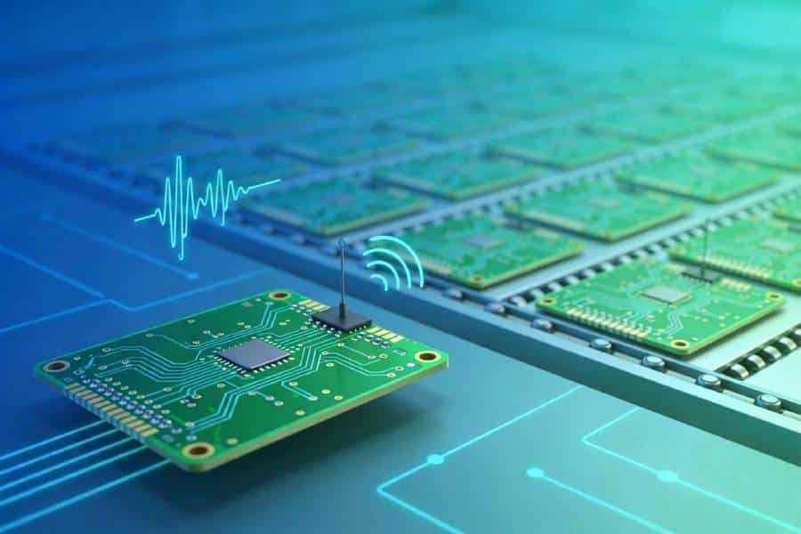
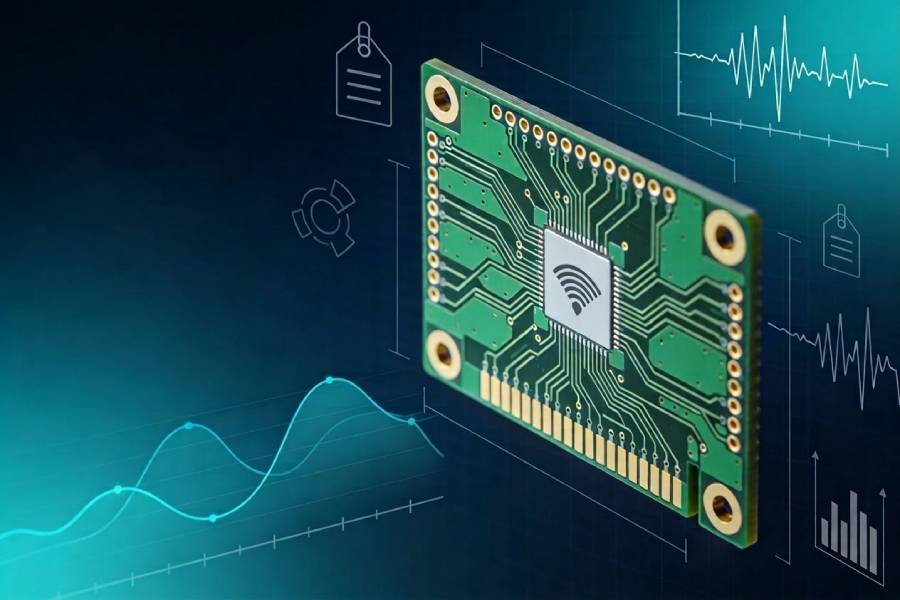
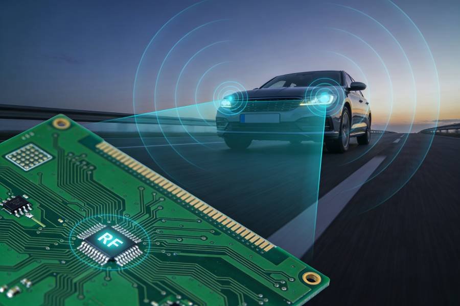
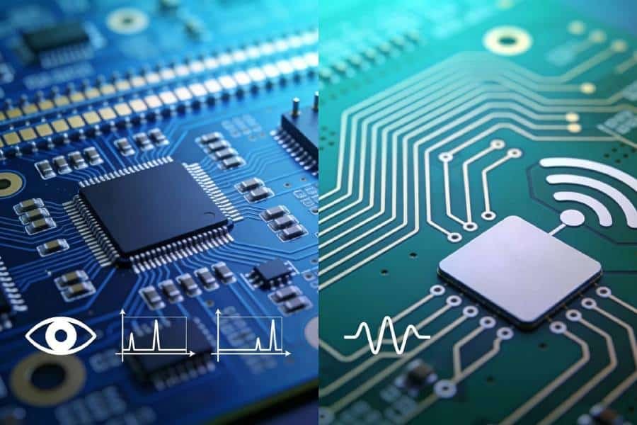
Engineers often use “high‑speed” and “high‑frequency” PCB design interchangeably, but they solve different problems. High‑speed PCBs focus on digital signal integrity and timing for fast edge‑rate interfaces, while high‑frequency PCBs focus on analog RF performance, loss, and impedance at GHz‑range carrier frequencies. This article explains the key differences, common overlaps, and how to pick the right materials, stackups, and manufacturing partner for each type of design.
High‑Speed vs High‑Frequency PCB: Key Differences, Design Rules, and Use Cases Read More »