Table of Contents
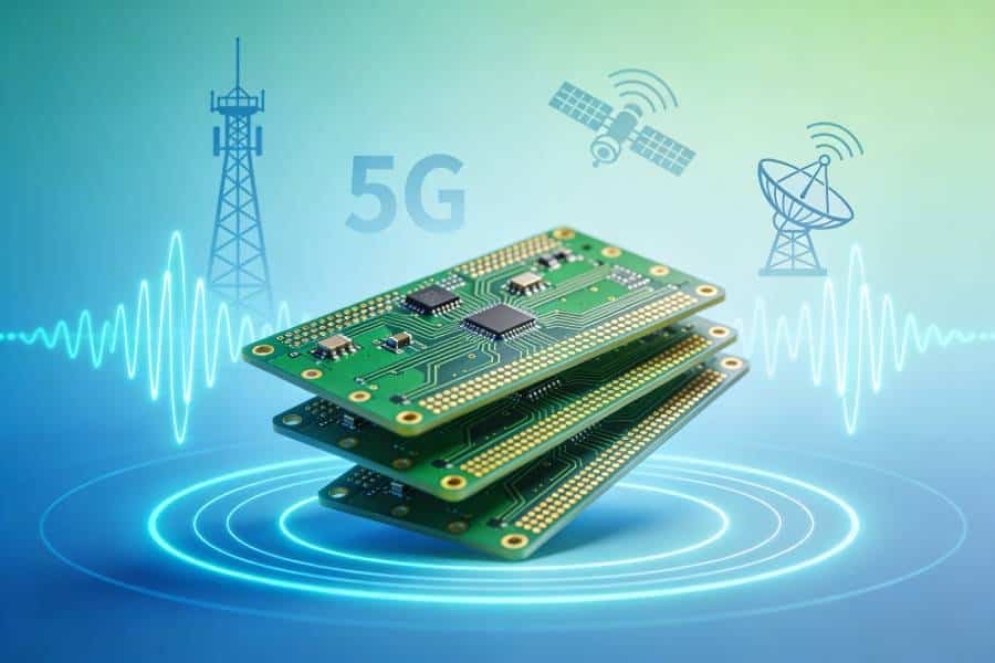
Satellite communication terminals—from large gateway earth stations to compact VSATs and user terminals—depend on carefully engineered RF front ends and control electronics built on specialized PCBs. Unlike generic RF boards, a satellite communication PCB must carry low‑loss RF paths across L, S, C, X, Ku, and Ka‑band links, interface cleanly with antennas and RF modules, and remain stable over wide temperature swings, mechanical stress, and long service lifetimes in remote or hard‑to‑service locations. When those PCBs sit on the satellite side of the link, the requirements tighten further: outgassing, radiation tolerance, and extreme thermal cycling conditions all have to be considered alongside RF performance.
This article focuses on practical high frequency PCB solutions for satellite communication terminals rather than abstract RF theory. We will look at how different satellite bands affect PCB material and stackup choices, what makes a high frequency PCB for satellite systems different from ordinary RF boards, and how to plan layouts, thermal paths, and manufacturing flows that meet reliability and quality standards for satcom applications. The goal is to give you a clear framework you can apply when working with your PCB manufacturer, so your next satellite communication PCB combines low loss and stable impedance with the robustness that satellite systems demand.
If you are looking for a manufacturing partner that understands both RF performance and space‑grade reliability, our high frequency PCB manufacturing services support satellite communication PCBs and high frequency PCBs for satellite systems, from material and stackup selection to volume production.
Satellite Communication Bands and PCB Implications
Satellite communication systems span multiple frequency bands—from L and S‑band up through C, X, Ku, and Ka‑band—and each band pushes different constraints onto the satellite communication PCB. Lower bands like L and S (roughly 1–4 GHz) are often used for mobile satellite services, navigation, TT&C, and moderate‑rate links, where path loss and weather effects are modest, but antenna sizes are larger and PCB loss budgets are somewhat more forgiving. In these bands, a high frequency PCB for satellite systems can often rely on low‑loss FR‑4 alternatives or hydrocarbon/ceramic laminates, with tighter focus on impedance control and stability than on absolute minimum insertion loss.
As you move into C and X‑band (around 4–12 GHz), PCB loss and dielectric consistency become more critical, especially in long feedlines, filter networks, and phased‑array or beamforming structures. Many ground terminals and some payload electronics in these bands adopt dedicated RF laminates with well‑controlled Dk and low Df to keep attenuation and phase errors within budget over temperature and across multiple channels. At Ku and Ka‑band (approximately 10–18 GHz and 26–40 GHz), which are widely used for broadband satellite internet, VSATs, and high‑throughput gateways, wavelengths shrink and bandwidths grow, so the PCB effectively becomes part of the RF front‑end and antenna feed network. Here, designers almost always use low‑loss PTFE‑based or advanced hydrocarbon/ceramic substrates with smooth copper, very tight impedance control, and careful layout to manage loss, dispersion, and radiation, especially in flat‑panel or phased‑array user terminals.
Whether you are building a ground terminal or hardware that rides on the satellite, starting from the frequency band and link budget is the most practical way to choose an appropriate material tier, stackup complexity, and level of RF integration for your satellite communication PCB.
Key Requirements for a Satellite Communication PCB
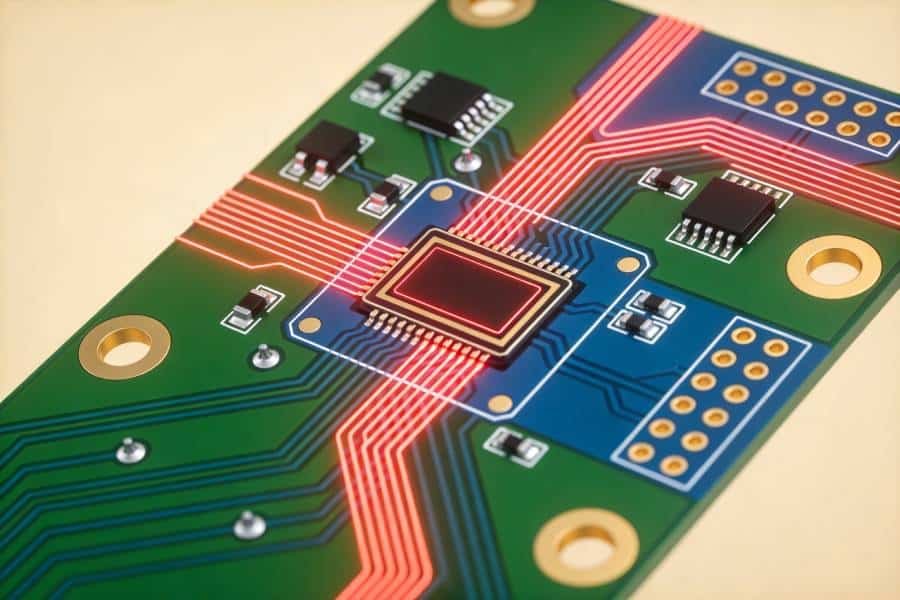
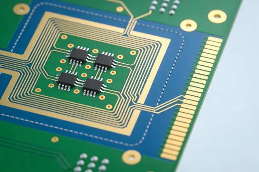
A satellite communication PCB has to deliver low‑loss, phase‑stable RF performance while also meeting aerospace‑level reliability requirements that go far beyond typical telecom hardware. Electrically, this means tight control of insertion loss, return loss, and impedance across wide operating bands and temperatures, with particular attention to phase stability for phased arrays, frequency converters, and high‑order modulation schemes. Small variations in dielectric constant, copper profile, or geometry can translate directly into link‑budget penalties, beam steering errors, or calibration drift in high frequency PCB designs for satellite systems.
Environmentally, satellite and satcom PCBs must withstand extreme temperature swings, launch vibration and shock, vacuum outgassing, and, for space hardware, long‑term radiation exposure. Boards may see temperatures from below –100 °C to above 120 °C, hundreds of thermal cycles, and multi‑g vibration during launch, so materials, vias, and solder joints must be chosen and qualified to avoid cracking, delamination, and fatigue over the mission life. In vacuum, convection cooling disappears and outgassing becomes a concern, so satellite communication PCBs rely on conduction into the structure and radiation to space for heat removal, and may use low‑outgassing laminates, conformal coatings, and assembly processes validated through thermal‑vacuum testing. For a high frequency PCB for satellite systems, process consistency and traceability in fabrication are also critical, because even small shifts in lamination, drilling, or plating can affect RF performance and long‑term stability across production lots.
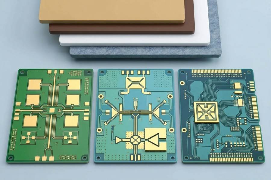
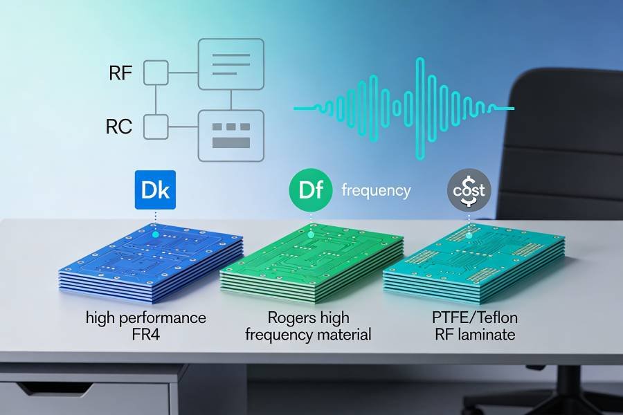
Material Choices for High Frequency PCB for Satellite Systems
Material selection for a satellite communication PCB starts with the operating band and environment, then narrows to laminates that can provide low loss, tight Dk control, and long‑term stability under thermal and mechanical stress. For many L/S‑band ground terminals and lower‑frequency payload electronics, low‑loss hydrocarbon/ceramic materials such as RO4000‑series laminates or thermoset‑based high frequency substrates can offer a good balance of insertion loss, manufacturability, and cost. These materials typically deliver Dk values in the 3.2–3.8 range with Df around 0.003–0.005 at 10 GHz, along with better temperature and moisture stability than enhanced FR‑4.
As designs move into Ku and Ka‑band for broadband satellite links and phased‑array terminals, PTFE‑based and ceramic‑filled PTFE laminates become increasingly attractive because they offer lower Df, tighter Dk tolerance, and smoother copper for reduced conductor loss. RT/duroid‑class materials, RO3000‑series laminates, and advanced thermoset/ceramic systems are commonly used here, with Dk values spanning roughly 2.2–10 depending on whether size reduction or ultra‑low loss is the priority. For example, RT/duroid 5880 offers a Dk of about 2.2 with extremely low loss, making it well suited to long RF feedlines and high‑Q structures, while higher‑Dk options such as RT/duroid 6010 or RO3035 enable more compact filters and couplers in tight payloads.
For space‑grade satellite communication PCBs and payloads, additional constraints apply: laminates must exhibit low outgassing, stable dielectric properties over extreme temperatures, and compatible CTEs with copper and attached components. Rogers highlights specific low‑outgassing versions of RT/duroid and RO3000/RO4000 materials for spacecraft, and thermoset‑based TMM‑series laminates are explicitly promoted for high‑reliability satellite communication systems, with Dk values in the z‑axis ranging from about 3.3 to over 12. In practice, many high frequency PCB designs for satellite systems use hybrid stackups that place PTFE‑based or TMM RF cores in the RF and antenna layers, while relying on polyimide or high‑temperature digital laminates for control logic and power management layers deeper in the stack.
When you need to turn these laminate options into a concrete, buildable stackup, our engineers can help you choose practical materials and thicknesses for your satellite communication PCB through our high frequency PCB material and stackup review service.
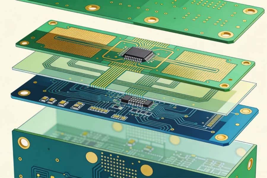
Stackup and Layout Strategies for Satellite Communication PCBs
Stackup and layout are where a satellite communication PCB really turns into part of the RF front end rather than just a carrier for components. The basic goals are to give every critical RF trace a clean reference plane, maintain consistent impedance over frequency and temperature, and control coupling so that sensitive RF paths are isolated from digital and power circuitry.
For most satellite terminals, four‑layer “entry‑level” RF stackups are quickly replaced by 6‑layer or higher structures that separate RF, digital, and power planes. A typical high frequency PCB for satellite systems might place RF traces and components on the top layer over a solid ground plane, use one or two inner layers for additional RF or high‑speed digital routing with adjacent planes, and reserve deeper layers for power distribution and digital I/O, all tied together with dense ground stitching vias. RF traces should be routed as controlled‑impedance microstrip or grounded coplanar waveguide, with uniform width, smooth bends or 45‑degree miters instead of sharp corners, and minimal via transitions to reduce reflections and radiation.
Grounding and shielding deserve special attention in satellite communication PCB layout. Continuous ground planes under RF regions provide low‑inductance return paths and help stabilize impedance, while via stitching along the edges of ground pours and between layers creates a low‑impedance RF cage around critical traces and antenna feeds. In compact satcom terminals and flat‑panel arrays, it is also important to enforce physical separation and, where needed, shielding between RF paths, local oscillators, high‑power amplifiers, and noisy digital clocks, so that spurious coupling does not degrade EVM, adjacent‑channel leakage, or beamforming accuracy.
High Frequency PCB for Satellite Systems: Thermal and Mechanical Design
Thermal design for a satellite communication PCB is fundamentally different from terrestrial hardware because convection cooling is minimal or non‑existent in vacuum; heat must leave components primarily through conduction into the board and structure, and then by radiation to space. For high‑power RF amplifiers, frequency converters, and digital processors on satcom boards, this typically means using dense thermal via arrays under hot devices, thick copper planes for lateral heat spreading, and solid mechanical interfaces to chassis or heat spreaders that act as radiators. Case studies on satellite communication PCBs show that combining thermal vias, 1–2 oz copper planes, external aluminum heat sinks, and high‑emissivity coatings can reduce device junction temperatures by tens of degrees compared to naive layouts.
Mechanically, satellite and launch environments subject PCBs to significant vibration and shock, so the high frequency PCB for satellite systems must be designed as a structural element, not just an electrical one. Board outlines, mounting hole patterns, and stiffeners should be chosen to avoid resonances in the dominant launch vibration bands, and heavy components should be placed near supports and, where needed, reinforced with underfill, staking, or mechanical brackets. Copper distribution and via placement also affect mechanical robustness—large unbalanced copper areas can drive warpage and local stress during thermal cycling, while poorly supported vias and pads are more prone to cracking under repeated load. By considering thermal paths and mechanical loading together early in the design, you can avoid re‑spins where otherwise acceptable RF layouts fail environmental tests late in the satellite communication PCB qualification process.
Reliability, Standards, and Manufacturing for Satellite Communication PCB
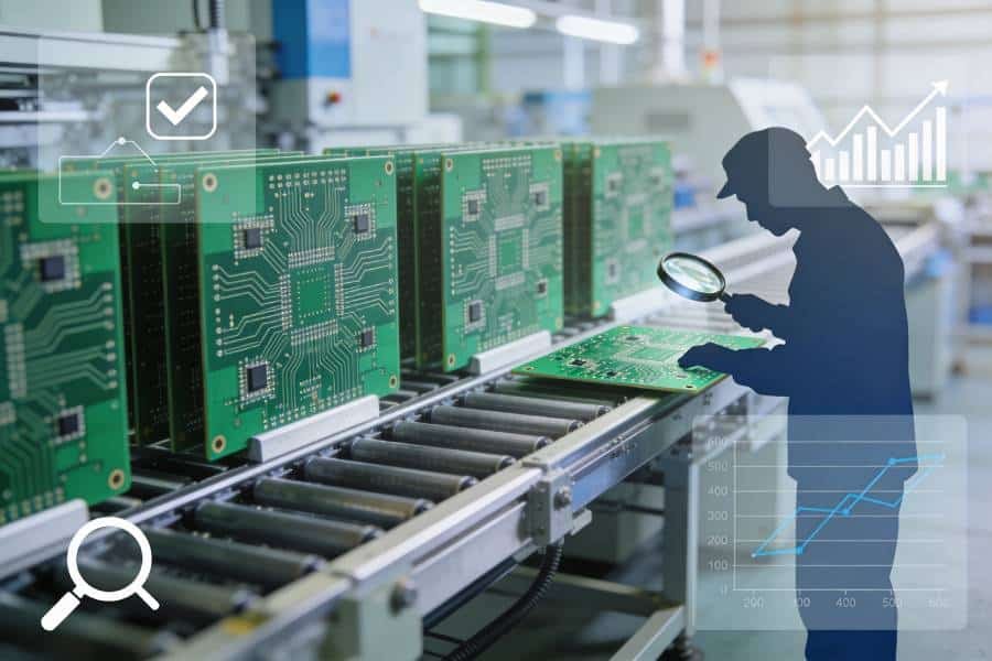
Compared with conventional RF hardware, a satellite communication PCB is normally built and qualified to aerospace‑class standards such as IPC Class 3 or 3A, often within an AS9100‑certified quality system. These standards drive requirements for tighter plating thickness, annular ring geometry, cleanliness, and dimensional tolerances, as well as strict traceability from raw laminate through finished assembly, because any latent defect can become a mission‑ending failure once hardware is on orbit or deployed in a remote ground station.
Manufacturing flows for high frequency PCB for satellite systems therefore emphasize controlled impedance processes, precise layer‑to‑layer registration, low‑loss surface finishes like ENIG or immersion silver, and 100% electrical testing of bare boards. Space‑grade builds typically add environmental screening and qualification at the board or assembly level, including thermal‑vacuum cycling, vibration and shock tests, and, for payload boards, radiation‑related evaluations tailored to the expected orbit and mission duration. When these standards and processes are integrated from the start—rather than bolted on at the end—designers and manufacturers can iterate toward satellite communication PCBs that meet both RF performance and long‑term reliability targets with fewer respins and schedule risks.
Practical Design Checklist for Satellite Communication Terminals
To turn these concepts into actionable steps, it helps to run each new design for a satellite communication PCB through a short checklist before locking the stackup and layout. The idea is to tie RF performance, environmental requirements, and manufacturing realities together early so that a high frequency PCB for satellite systems can pass both lab tests and qualification campaigns with minimal rework.
1. Clarify the system context
- Is this PCB for a ground terminal, gateway, user terminal, or on‑board satellite payload?
- Which bands are used (for example L/S vs Ku/Ka) and what are the link‑budget and EVM targets?
- What is the expected lifetime and service environment (indoor, outdoor remote site, LEO/GEO orbit)?
2. Choose an appropriate material tier
- For L/S/C/X‑band ground hardware, shortlist low‑loss hydrocarbon/ceramic laminates; for Ku/Ka‑band and space payloads, move toward PTFE‑based or TMM‑class materials.
- Check Dk/Df stability over temperature, moisture absorption, outgassing (for space), and CTE compatibility.
- Confirm that your PCB fabricator stocks these laminates and has experience processing them for RF applications.
3. Plan the stackup and RF layout
- Use at least 6 layers for complex terminals, with RF layers adjacent to solid ground planes and separate layers for digital and power.
- Route RF as controlled‑impedance microstrip or CPWG with minimal via transitions and keep critical RF paths short and direct.
- Add via stitching and ground fences around sensitive RF regions and along board edges to control radiation and coupling.
4. Address thermal and mechanical constraints
- Define clear thermal paths from hot components into copper planes, mounting points, and external heat sinks or radiators.
- Consider vibration and shock during launch or transport when choosing board thickness, mounting scheme, and placement of heavy components.
5. Align with reliability standards and manufacturing
- Decide early whether the build must meet IPC Class 3/3A, space‑grade, or other aerospace standards, and design for those rules from the start.
- Work with your fabricator and assembler to define test vehicles, coupons, and environmental screenings (thermal‑vacuum, vibration, radiation where applicable) before qualification builds.
Conclusion: Building Robust High Frequency PCBs for Satellite Systems
Designing a satellite communication PCB means meeting demanding RF performance targets and aerospace‑class reliability at the same time. The combination of low‑loss, tightly controlled laminates, RF‑aware stackups, disciplined layout, and careful thermal and mechanical design is what turns a promising satcom concept into a high frequency PCB for satellite systems that survives real‑world deployment on the ground or in orbit.
In practice, success comes from starting with the satellite bands and service environment, selecting materials and stackups your manufacturer can actually build, and integrating reliability standards and environmental testing into the plan from the first prototypes—not as a last‑minute hurdle before launch. When designers and PCB manufacturers work together this way, satellite communication PCBs become stable, repeatable platforms that you can reuse and scale across multiple terminals and missions with fewer respins and qualification surprises.
When your next satellite communication terminal or payload design is ready to move beyond the lab, our end‑to‑end high frequency PCB manufacturing and assembly services for satellite systems can help you bridge the gap from prototype stackups to qualified production hardware.