Table of Contents
Introduction to PCB Copper Foils in High-Frequency Designs
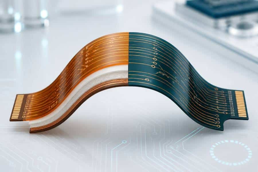
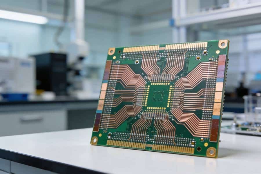
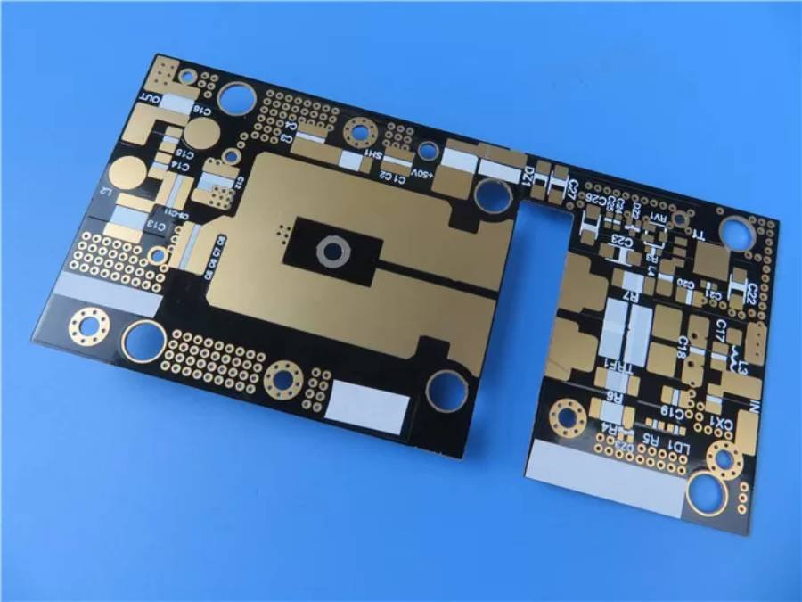
In high-frequency and high-speed PCB designs, material selection is critical to minimizing signal loss, maintaining impedance stability, and ensuring reliable performance. The PCB industry has invested significant effort into developing materials that reduce signal attenuation, particularly for applications operating at frequencies like 5 GHz (e.g., WiFi) or higher. One key factor in these designs is the type and roughness of the copper foil used in the PCB stackup.
Copper roughness directly influences signal integrity by contributing to impedance deviations and insertion loss, observable in Time-Domain Reflectometry (TDR) measurements. While smoother copper may seem like the obvious choice for minimizing losses, the question remains: How smooth does your copper foil need to be? Are there ways to mitigate losses without always opting for ultra-smooth copper? This article explores the various types of PCB copper foils, their manufacturing processes, and practical considerations for high-frequency designs.
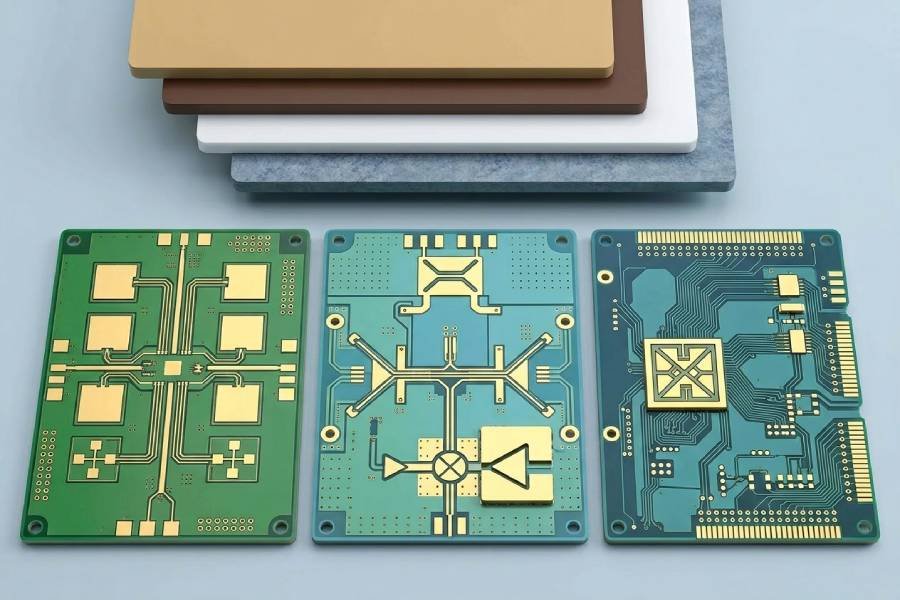
Understanding Copper Foil Types for PCBs
When discussing copper in PCB manufacturing, the focus is typically on surface roughness rather than the type of copper itself. Different deposition and processing methods produce copper foils with varying roughness levels, which can be distinguished under a scanning electron microscope (SEM). For high-frequency applications (typically 5 GHz and above), selecting the appropriate copper foil is crucial. Below, we outline the main types of copper foils used in PCB manufacturing and their implications for high-frequency designs.
1. Electrodeposited Copper Foil
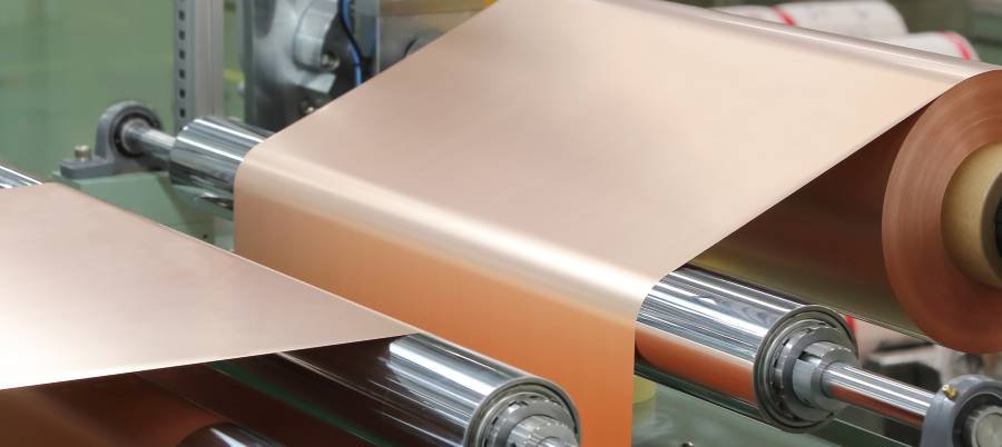
Electrodeposited copper foil is produced through an electrochemical process where a rotating drum passes through an electrolyte solution, allowing copper to “grow” on the drum’s surface. As the drum rotates, a continuous copper sheet forms, which is later laminated onto a dielectric substrate, such as fiberglass.
- Process: The copper surface facing the drum (drum side) is smooth, matching the drum’s surface roughness. The opposite side (open side) is significantly rougher.
- Application in PCBs: The rough side is bonded to the dielectric material, while the smooth drum side is exposed. To ensure adhesion in standard PCB lamination processes, the drum side undergoes chemical roughening, such as plasma etching, to bond effectively with the next layer in the stackup.
- Use Case: Electrodeposited copper is widely used in standard PCB manufacturing due to its cost-effectiveness and versatility.
2. Surface-Treated Copper Foil
Surface-treated copper foils are electrodeposited foils that undergo additional processing to modify their surface properties, primarily to enhance adhesion to dielectric materials and prevent corrosion. These foils are commonly referred to as “back-treated” foils, though other variations exist.
- Process: A thin secondary copper coating is applied to the smooth drum side via an additional electrolyte bath, followed by a barrier seed layer and an anti-tarnish film. This treatment increases surface roughness to improve adhesion while acting as an anti-oxidation layer.
- Types of Surface-Treated Copper:
- High-Temperature Elongation (HTE) Copper Foil: Meets IPC-4562 Grade 3 standards and includes an oxidation barrier to prevent corrosion during storage.
- Double-Treated Foil: Both sides of the copper foil are treated, sometimes called drum-side treated foil, enhancing adhesion on both surfaces.
- Resistive Copper: Features a metal coating on the matte side, which is then roughened to the desired level. This is not always classified as a surface-treated foil but serves similar purposes.
- Advantages: The treated surface is ready for lamination without additional roughening, simplifying the manufacturing process.
3. Rolled and Annealed Copper Foil
Rolled and annealed (RA) copper foil is produced by passing a copper sheet through rollers to achieve the desired thickness via cold rolling. The resulting foil’s roughness depends on rolling parameters, such as speed and pressure.
- Characteristics: RA copper can achieve very low roughness, often exhibiting visible striations on the surface. This makes it particularly suitable for high-frequency applications where minimal signal loss is critical.
- Comparison to Electrodeposited Copper: RA copper is generally smoother than electrodeposited copper, reducing skin effect losses at high frequencies.
4. Low-Profile Copper Foil
Low-profile (LP) copper foils are electrodeposited foils processed to achieve very low surface roughness while maintaining sufficient adhesion to the substrate. These foils are often patented and categorized based on their roughness levels:
- Ultra-Low Profile (ULP): Extremely smooth surfaces for minimal signal loss.
- Very Low Profile (VLP): Slightly rougher than ULP but still optimized for high-frequency designs.
- Low Profile (LP): Average roughness of approximately 1 micron, balancing adhesion and signal performance.
- Process: Micro-roughness treatments are applied to electrodeposited copper to reduce average surface roughness while ensuring compatibility with standard PCB manufacturing processes.
- Use Case: Low-profile copper is ideal for high-frequency designs requiring minimal signal attenuation, such as 5G, radar, and high-speed digital circuits.
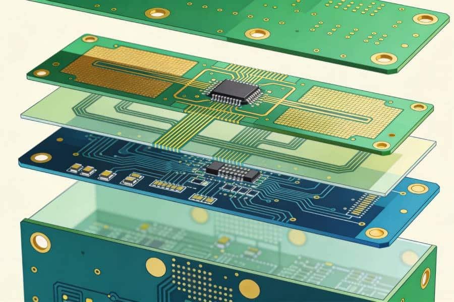
Copper Roughness and Its Impact on High-Frequency Designs
Copper roughness significantly affects signal propagation in high-frequency PCBs due to the skin effect, where high-frequency signals travel primarily along the conductor’s surface. Rougher surfaces increase resistance and signal loss, leading to:
- Increased Insertion Loss: Rough copper surfaces scatter signals, reducing signal strength over distance.
- Impedance Deviations: Variations in copper roughness can cause impedance mismatches, visible in TDR measurements.
- Signal Distortion: Rough surfaces contribute to phase distortions, impacting signal integrity in high-speed designs.
While ultra-smooth copper (e.g., ULP or RA copper) minimizes these issues, it comes at a higher cost and may not always be necessary. Designers can mitigate losses through:
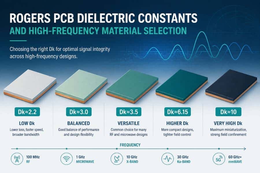
- Material Selection: Choose dielectrics with low dissipation factor (Df) and dielectric constant (Dk) to complement copper foil choices. Always verify Dk values in material datasheets, as they can vary depending on frequency.
- Trace Geometry Optimization: Wider traces and shorter signal paths can reduce losses, even with rougher copper.
- Simulation Tools: Use electromagnetic simulation software to model signal behavior and optimize stackup design.
Practical Considerations for Choosing Copper Foils
When selecting copper foils for high-frequency PCB designs, consider the following:
- Frequency Range: For applications below 5 GHz, standard electrodeposited copper may suffice. For 5G, mmWave, or high-speed digital designs, low-profile or RA copper is preferred.
- Cost vs. Performance: Ultra-smooth copper foils like ULP or VLP are expensive. Evaluate whether the performance benefits justify the cost for your application.
- Manufacturing Compatibility: Ensure the copper foil is compatible with your PCB fabrication process. Surface-treated and low-profile foils are designed for standard lamination processes, while RA copper may require specialized handling.
- Datasheet Analysis: Pay close attention to copper roughness specifications (e.g., Ra or Rz values) and Dk/Df values in material datasheets. For deeper insights into Dk specifications, refer to industry discussions, such as Rogers’ podcast with John Kunrod.
Conclusion
Selecting the right copper foil for high-frequency PCB designs is a balance between performance, cost, and manufacturing feasibility. Electrodeposited copper offers versatility for standard applications, while surface-treated and low-profile foils cater to high-frequency needs with improved adhesion and reduced signal loss. Rolled and annealed copper provides the smoothest surfaces for critical applications but at a higher cost. By understanding the trade-offs and leveraging material datasheets, designers can optimize their PCB stackups for reliable high-frequency performance.