Table of Contents
As a team at JHYPCB, your reliable PCB manufacturer based in China, we’re passionate about sharing practical knowledge that helps engineers and designers create better electronics. Our expertise covers a wide range of PCB manufacturing services, including prototypes, single-sided, double-sided, multilayer, rigid, flexible, and rigid-flex PCBs. In this post, we’ll focus on copper foil—a key element in the PCB fabrication process—and break down its role, types, design considerations, and selection tips. If you’re designing circuits or troubleshooting builds, these insights can make a real difference in your project’s success.
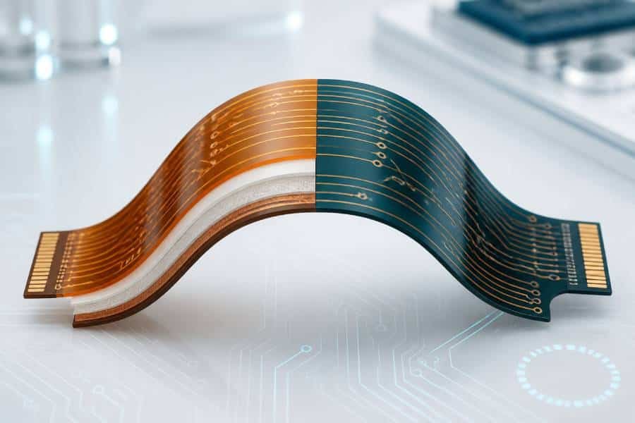
Demystifying Copper Foil: The Conductive Core of PCBs
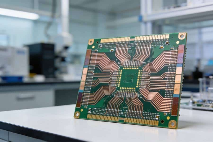
Copper foil is essentially a thin sheet of high-purity copper, often exceeding 99.7% purity, with low surface oxidation to ensure strong bonding to various substrates like metals or insulating materials. In PCB manufacturing, it forms the conductive traces that carry electrical signals and power, while also providing electromagnetic shielding and antistatic protection to keep your circuits running smoothly.
Typically supplied in rolls, copper foil comes in thicknesses ranging from 1/3 oz/ft² (about 12 μm or 0.47 mil) to 2 oz/ft² (70 μm or 2.8 mil). This weight measurement—ounces per square foot—helps determine the right thickness for your design needs, whether it’s handling high currents or fitting fine-pitch components in multilayer PCBs.
You’ll find copper foil in several varieties:
- Self-adhesive copper foil, great for quick prototypes or repairs.
- Single-sided copper foil, applied to one side of the board for simpler layouts.
- Double-sided copper foil, used on both sides to support more complex routing in advanced designs.
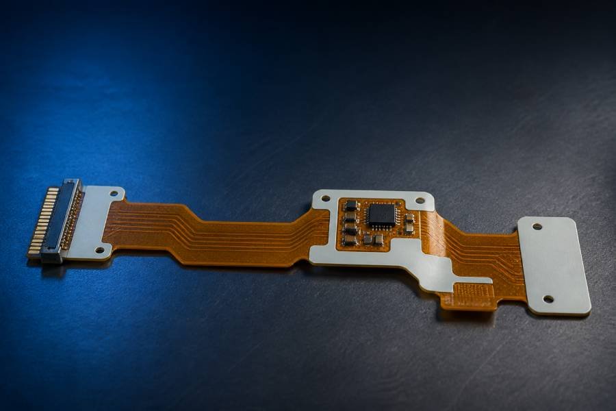
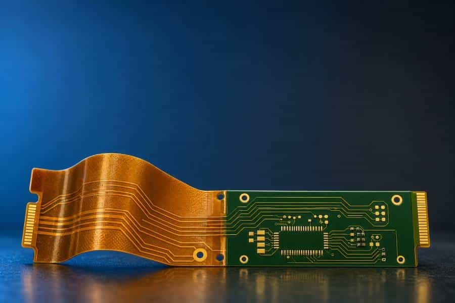
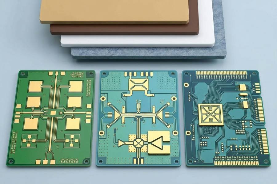
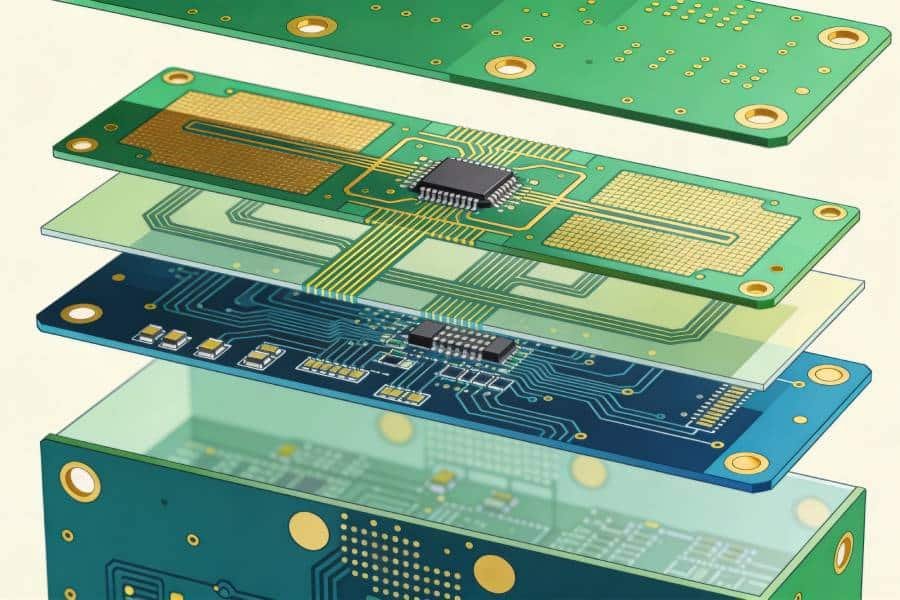
In the fabrication process, manufacturers laminate copper foil onto base materials such as FR-4, polyimide, PTFE, or ceramic. For multilayer boards, it’s pressed with prepregs or cores, and outer layers often get an extra plating layer of 18-30 μm for added strength. This is especially crucial in high-density interconnect (HDI) PCBs, where resin-coated copper (RCC) enables precise microvias and reliable performance.
One practical tip: When working with copper foil thickness in multilayer PCBs, always factor in signal integrity—thinner foils reduce capacitance but may not handle heavy loads, so balance is key for optimal results.
Why Copper Foil is Indispensable in Modern PCB Production
The electronics boom has made electronic-grade copper foil (with thicknesses from 5 μm to 105 μm) a cornerstone material. It’s widely used in everything from communication devices and automotive electronics to lithium-ion batteries and consumer gadgets like TVs, phones, and gaming consoles. Its high conductivity and versatility drive efficiency in these applications.
Industrially, copper foil splits into two main categories:
- Rolled annealed (RA) copper foil, prized for its ductility and ideal for flexible PCBs where bending is involved.
- Electrodeposited (ED) copper foil, a more budget-friendly option with straightforward production, commonly used in rigid PCBs.
Choosing between electrodeposited vs rolled annealed copper foil depends on your project’s demands—RA for flexibility in wearables, ED for cost-effective standard boards. As the industry evolves, these materials continue to influence design trends, especially with rising demands for smaller, more efficient circuits.
Essential Design Rules for Copper Foil in PCBs
PCBs are everywhere—you’re probably interacting with one right now in your device. But getting the design right starts with how you handle copper foil.
At its core, a PCB is a glass-reinforced plastic substrate where copper traces replace traditional wires to guide electrical flow to components. For single-layer PCBs, copper foil covers one side, leaving the other for parts—perfect for basic setups. Double-layer PCBs use copper on both sides, allowing intricate paths without crossings, which is essential for more demanding electronics.
Don’t forget the supporting layers: Solder masks add color (think classic green or custom purple) and protect the copper, making connections easier to follow. Silkscreen layers provide labels with letters and numbers for quick reference during assembly or debugging.
A key rule: In multilayer designs, ensure traces don’t overlap to avoid shorts, and calculate minimum widths based on current—say, 0.25 mm for 1A signals—to prevent overheating. These guidelines help create robust boards that perform reliably under real-world conditions.
Selecting the Optimal Copper Foil Material: A Step-by-Step Guide
Picking the right copper foil isn’t guesswork; it’s a methodical process to match your PCB’s requirements.
Start with the substrate: This dielectric layer, often made from epoxy resins and fiberglass, needs to align with specs like glass transition temperature (Tg) for heat resistance.
Next, consider lamination: Done under high pressure, it bonds everything together, impacting thermal expansion, shear strength, and overall durability—critical for maintaining electrical flow.
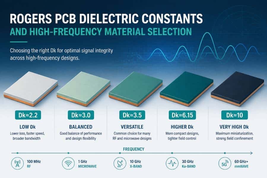
Weigh factors like current capacity, thermal needs, and application type. For high-frequency PCBs, low-oxygen copper foil minimizes signal loss. In flexible designs, prioritize ductility to handle repeated bends without cracking.
Emerging trends, like sustainable copper sourcing, are also worth noting as the industry pushes for greener manufacturing without compromising quality.
FAQ: Common Questions on Copper Foil in PCB Manufacturing
What's the link between copper foil weight and thickness?
It’s directly related—1 oz/ft² equals about 35 μm, influencing how much current your traces can carry in multilayer setups.
How does copper foil help with EMI shielding?
Its conductive properties block electromagnetic interference, vital for sensitive devices like medical equipment or comms gear.
Can copper foil be recycled in PCB production?
Yes, and with growing eco-awareness, recycled options are becoming more viable for reducing environmental impact.
In wrapping up, copper foil truly is the foundation of effective PCB manufacturing, enabling conductivity, durability, and innovation in your designs. If you’d like to discuss how it fits into your next project or need quotes on our PCB manufacturing services, drop us a line at sales@pcbjhy.com. We’re here to help bring your ideas to life with expertise you can trust.