Table of Contents
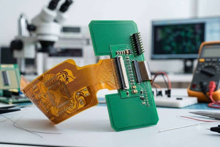
As a leading PCB manufacturer based in China, at JHYPCB, we’ve been helping engineers and designers bring their ideas to life for years. Whether it’s crafting high-quality PCB prototypes, fabricating single-sided, double-sided, or multilayer boards, or handling full turnkey PCB assembly services—including SMT, THT, hybrid technologies, component sourcing, and even SMT stencils—we know that every detail matters. One question we hear often from clients working on flexible PCBs or rigid-flex designs is: “Will my board hold up under repeated bending if I choose the wrong copper foil?” It’s a valid concern, especially when flexibility and reliability are key to your project’s success.
In the world of PCB manufacturing, copper foil is the backbone of conductivity and durability. But not all copper is created equal. Today, we’re diving deep into the two primary types: RA copper (rolled annealed) and ED copper (electrodeposited). If you’ve ever wondered about “RA copper vs ED copper in flexible PCBs” or how these materials affect signal integrity in high-frequency applications, this guide is for you. Drawing from our hands-on experience at JHYPCB, where we’ve produced thousands of flexible and rigid-flex PCBs, we’ll break it down step by step. We’ll go beyond basic overviews—like those you might find in industry articles—to provide practical insights, real-world examples, and tips to optimize your designs. By the end, you’ll know exactly when to choose one over the other, ensuring your PCB assembly process runs smoothly and your final product stands out in the market.
Let’s get started.
What is ED Copper (Electrodeposited Copper Foil)?
Electrodeposited copper, or ED copper, is one of the most common materials in PCB fabrication. It’s produced through an electrolysis process where copper ions are deposited onto a rotating drum cathode in an electrolytic bath. This method allows for precise control over thickness, making it versatile for various applications.
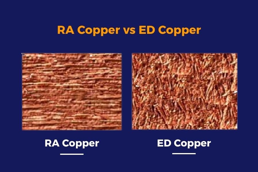
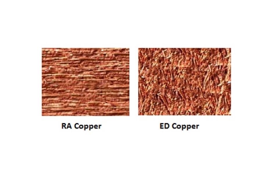
At its core, ED copper features a vertical, columnar grain structure. This means the copper crystals grow perpendicular to the surface, which can lead to a somewhat brittle material under stress. Surface roughness is another key trait—standard ED foils often have a higher profile compared to other types, which helps with adhesion during lamination in multilayer PCBs but can introduce challenges elsewhere.
From our experience at JHYPCB, ED copper shines in cost-sensitive projects. It’s widely available and affordable, making it ideal for high-volume production of rigid PCBs or even some flexible ones where extreme bending isn’t required. For instance, in consumer electronics like smartphones or basic wearables, ED copper handles fine-line etching well, supporting trace widths down to 3 mils without issues.
However, it’s not without drawbacks. The vertical grains make ED copper less ductile, so it might crack after fewer flex cycles—typically around 100,000 in dynamic applications, based on IPC-6013 standards we’ve tested against. In high-frequency circuits, the rougher surface can cause signal loss due to skin effect, where currents travel on the outer layer. We’ve seen this in prototypes where clients initially opted for ED to cut costs, only to rework for better performance.
That said, don’t dismiss ED copper outright for flexible designs. With careful control—such as limiting plated through-hole (PTH) additions and using thinner foils (e.g., 1/2 oz)—it performs admirably in lightweight, high-cycle consumer apps. At JHYPCB, we’ve successfully used ED copper in turnkey PCB assembly for flexible prototypes in IoT devices, where weight and cost were priorities.
What is RA Copper (Rolled Annealed Copper Foil)?
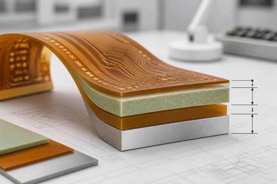
On the flip side, rolled annealed copper, or RA copper, takes a different path to production. It starts with pure copper ingots that are rolled into thin sheets and then annealed (heated and cooled) to relieve stresses and refine the grain structure. This results in elongated, horizontal grains that align parallel to the surface, giving RA copper its signature ductility.
The smooth surface is a standout feature—much lower roughness than ED, which minimizes signal attenuation in high-speed or RF applications. We’ve leveraged this at JHYPCB for clients in aerospace and automotive sectors, where boards must endure vibrations and thermal cycles without failing.
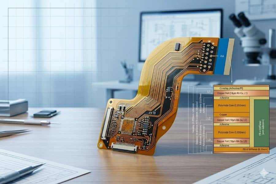
RA copper has been a staple in flexible PCB manufacturing for decades, and for good reason. Its grain structure allows for exceptional fatigue resistance, often surviving over a million flex cycles in dynamic setups. This makes it perfect for rigid-flex PCBs that combine stiff and bendable sections, like those in medical devices or foldable gadgets.
Of course, excellence comes at a price. RA copper is more expensive due to the mechanical rolling process and isn’t as readily available in ultra-thin variants (below 9 microns). Processing it requires specialized equipment, which is why we at JHYPCB invest in advanced fabrication lines to handle it seamlessly during PCB assembly.
In one recent case study, a client approached us for a rigid-flex PCB prototype for a wearable fitness tracker. We recommended RA copper for the flex areas, and after SMT assembly and testing, the board withstood 1.5 million bends—far surpassing their specs. This highlights why “rolled annealed copper foil benefits” and “RA copper for flexible circuits” are hot topics in PCB design forums.
Key Differences Between RA Copper and ED Copper
To make this comparison crystal clear, let’s break it down side by side. While both foils conduct electricity effectively, their microstructures and properties lead to distinct performance profiles. Here’s a quick table summarizing the essentials, based on our lab tests and industry benchmarks like IPC standards:
| Property | RA Copper (Rolled Annealed) | ED Copper (Electrodeposited) |
|---|---|---|
| Grain Structure | Horizontal, elongated grains for high ductility | Vertical, columnar grains; more brittle |
| Flexibility | Excellent; up to 1M+ flex cycles in dynamic apps | Good for static; ~100K cycles max in flex |
| Surface Roughness | Low (smooth); ideal for high-frequency signals | High (rough); better adhesion but higher losses |
| Thickness Range | Typically 18-70 microns; supports heavier weights | 9-105 microns; versatile for thin foils |
| Cost | Higher; premium for reliability | Lower; economical for volume production |
| Applications | Flexible/rigid-flex PCBs, high-speed circuits | Rigid PCBs, cost-sensitive flex, fine-pitch |
| Signal Integrity | Superior; low insertion loss | Adequate; potential issues in RF/high-speed |
Diving deeper, the grain structure is the real game-changer. RA’s aligned grains distribute stress evenly during bending, reducing crack propagation—crucial for “flexibility in PCB copper types.” ED’s vertical setup, while strong in compression, falters under tension, which we’ve observed in failure analysis during PCB prototyping.
Surface characteristics also play a big role. In high-frequency designs (think 5G or microwave), RA’s smoothness cuts down on dielectric losses, improving overall efficiency. We’ve quantified this in our facility: RA foils show 10-20% less signal degradation compared to ED in tests at 10 GHz.
Cost and availability? ED wins for quick-turn prototypes, but RA is essential for heavy-current apps (over 1 oz copper weight), where dynamic flex is non-negotiable. A common myth we bust: You don’t have to “fear” ED in flex circuits if you control factors like bend radius and plating thickness. But for ultimate longevity, RA is our go-to recommendation at JHYPCB.
Searching for “RA copper vs ED copper differences” or “copper foil grain structure comparison”? This table and analysis should give you the edge in your next design review.
Applications and When to Choose Each Type
Choosing between RA and ED copper isn’t just about specs—it’s about matching the material to your project’s demands. In flexible PCBs for wearables or medical implants, RA copper excels due to its bend endurance. We’ve assembled hundreds of such boards at JHYPCB, where clients need boards that fold repeatedly without trace fractures.
For rigid PCBs in consumer gadgets or industrial controls, ED copper is often sufficient and more budget-friendly. It pairs well with our SMT stencil services for precise soldering in high-density layouts.
In rigid-flex hybrids—common in drones or automotive infotainment—RA handles the flex transitions, while ED can cover rigid sections to balance costs. High-frequency apps? RA all the way for “smooth surface copper in high-frequency PCBs,” as it preserves signal quality.
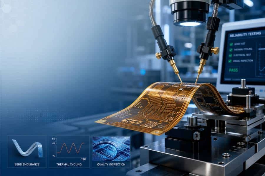
Our advice: Factor in your assembly process. For turnkey PCB assembly, specify RA if dynamic flex is key; use ED for prototypes to iterate quickly. Tools like Altium or KiCad let you annotate foil types early. And always test per IPC-TM-650 for flex life— we’ve got the equipment at JHYPCB to help with that.
Long-tail tip: If you’re querying “best copper foil for turnkey PCB assembly in flexible prototypes,” start with your end-use environment.
Advantages, Disadvantages, and Cost Considerations
To wrap this up before our conclusion, here’s a balanced pros/cons list:
RA Copper Advantages:
- Superior flexibility and fatigue resistance for dynamic applications.
- Better signal integrity in high-speed designs.
- Supports heavier copper weights for power-hungry circuits.
RA Copper Disadvantages:
- Higher material and processing costs.
- Limited availability in very thin forms.
ED Copper Advantages:
- Cost-effective and widely sourced.
- Excellent for fine-pitch etching and multilayer adhesion.
- Versatile for both rigid and light-flex needs.
ED Copper Disadvantages:
- Lower flex cycles; risk of cracking in repeated bends.
- Potential signal losses from surface roughness.
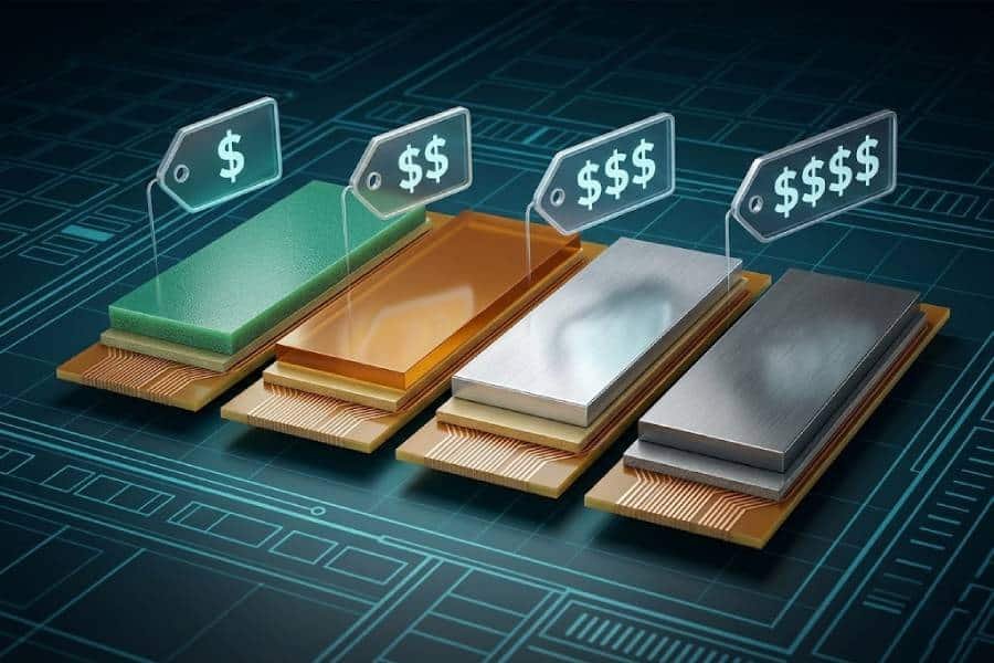
On costs: While ED keeps prototyping affordable (think under $100 for small runs), RA adds value through reduced failures and rework. At JHYPCB, we emphasize sustainability too—RA’s durability means less waste, aligning with our eco-friendly manufacturing practices. Always weigh procurement: Can you source it affordably without pricing your product out of the market?
Conclusion
In summary, the choice between RA copper and ED copper boils down to your PCB’s flexibility requirements, budget, and performance goals. RA stands out for demanding flexible and rigid-flex applications, offering unmatched durability and signal quality. ED, meanwhile, delivers efficiency and cost savings for standard or static designs. At JHYPCB, we’ve seen both transform projects—from ED in budget IoT prototypes to RA in high-reliability automotive boards.
Ready to apply this to your next PCB manufacturing or assembly project? Contact our team at sales@pcbjhy.com for a free quote on custom prototypes, full turnkey services, or expert advice on copper foil selection. We’re here to make your designs flex—literally and figuratively.
For more insights, check out our previous post on PCB materials. And remember, optimizing for “choosing RA or ED copper for PCB design” starts with partners like us who prioritize quality and innovation.