


6 Layer PCB Manufacturing & Fabrication | China Manufacturer
China-based 6 layer PCB manufacturer providing advanced stackup design, controlled impedance and quick-turn multilayer PCB fabrication for global OEMs.
- Engineering-driven stackup & DFM support for high-speed, RF and power electronics designs.
- Reliable quality with IPC-compliant processes, 100% electrical testing and strict impedance verification.
- Quick-turn prototypes and small to medium batch production with competitive pricing from China.
- Global delivery experience, with a strong customer base in North America and Europe.
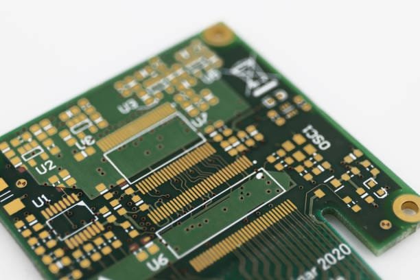
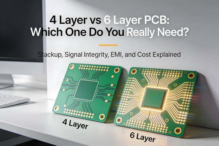
What Is a 6 Layer PCB?
A 6 layer PCB is a multilayer printed circuit board composed of six copper layers laminated with insulating materials to form a compact, high‑density interconnect structure.
By adding extra internal signal and plane layers, a 6 layer board improves signal integrity, power distribution and EMI performance compared to 2‑layer and 4‑layer designs.
It offers a balanced combination of electrical performance and cost, making it a popular choice for mid‑to‑high‑end electronic products.
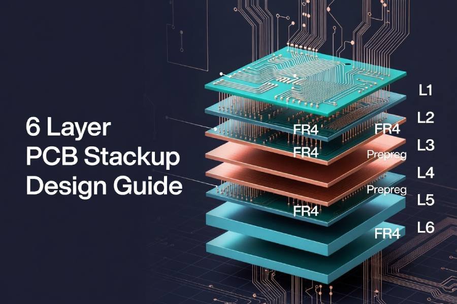
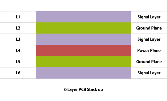
Typical 6 Layer PCB Structure
In a typical 6 layer PCB stackup, outer layers are used for component mounting and routing, while inner layers are dedicated to ground, power and high‑speed signal routing.
A common 6 layer stackup example is: Top (signal) – GND – Inner signal – PWR – GND – Bottom (signal), providing short return paths, stable power and effective EMI shielding.

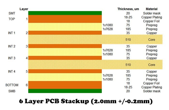
Fig.1
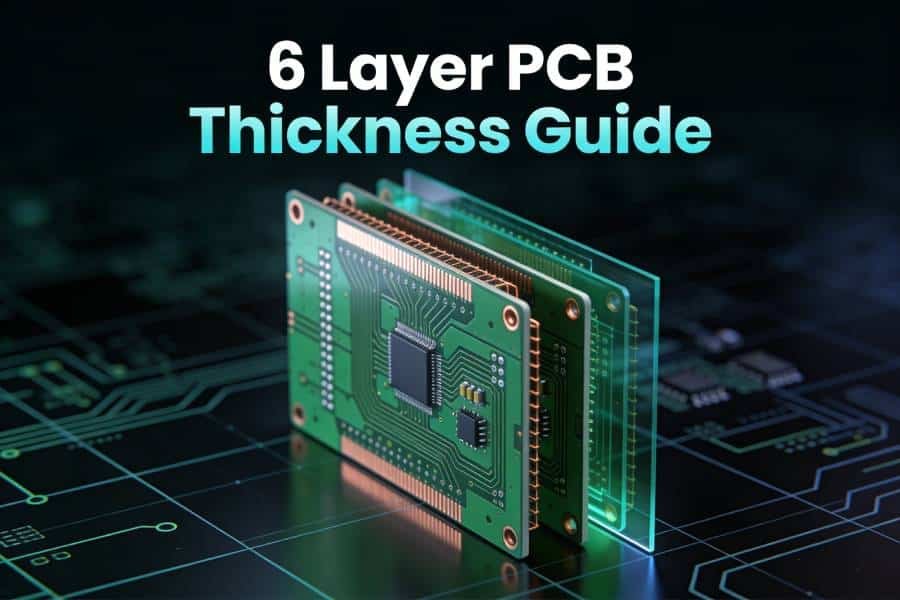
standard 1.6mm 6 Layer PCB Stackup and Thickness
Related Reading: Standard PCB Thickness—All You Need To Know
Why Use a 6 Layer PCB?
- Higher density & smaller size – Extra routing layers allow more components and complex interconnects in a compact footprint.
- Better signal integrity – Dedicated ground planes and well‑planned stackups reduce crosstalk, reflections and noise in high‑speed and RF designs.
- Improved power integrity – Internal power planes provide low‑impedance power distribution and better decoupling for sensitive ICs.
- Enhanced EMI/EMC performance – Inner planes and shielding help meet stringent EMI/EMC requirements in modern electronic devices.
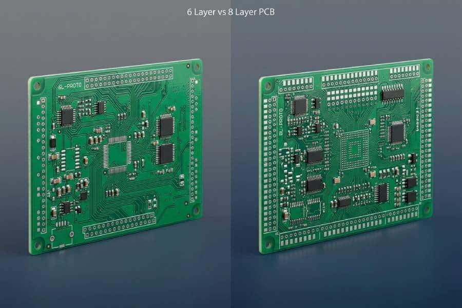
- Balanced cost vs. performance – More capable than 4‑layer boards but cheaper and less complex than many 8‑layer designs.
When Do You Need a 6 Layer PCB?
A 6 layer PCB is typically selected when a design requires multiple high‑speed interfaces, dense BGAs, controlled impedance routing or stricter EMI performance than a 4 layer board can offer.
It is widely used in communication equipment, embedded systems, networking devices, industrial control and other performance‑critical applications.
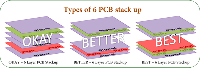
Typical 6 Layer PCB Stackups
The layer stackup is the foundation of any 6 layer PCB, directly affecting signal integrity, power integrity, EMI/EMC performance and manufacturability.
By choosing the right 6 layer stackup, designers can balance routing density, impedance control and cost for different applications.
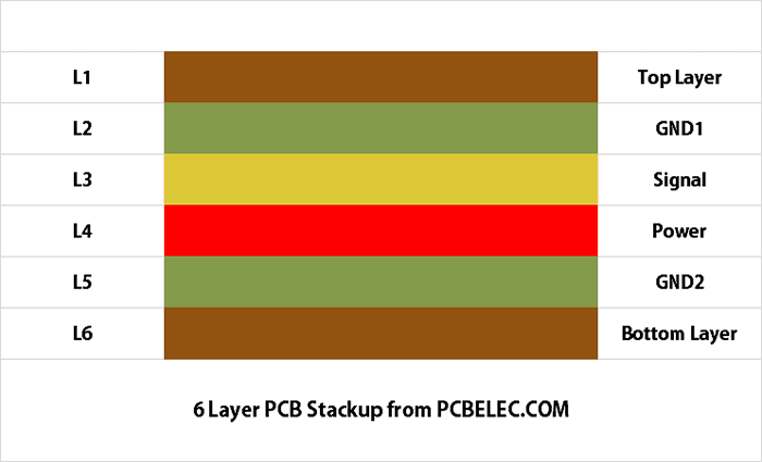
Standard 6 Layer Stackup for High‑Speed Digital
A widely used 6 layer PCB stackup for high‑speed digital designs is:
Top (Signal) – GND – Inner Signal – PWR – GND – Bottom (Signal).
- Every signal layer is closely coupled to an adjacent ground or power plane, providing short, low‑inductance return paths.
- Dedicated power and ground planes improve power integrity and help reduce switching noise and EMI.
- Suitable for many high‑speed interfaces such as USB, HDMI, DDR and high‑speed serial links in compact products.
EMI‑Optimized 6 Layer Stackup
For products that must meet strict EMI/EMC standards, a more shielded 6 layer stackup can be used, for example:
Signal – GND – Signal – PWR – Signal – GND.
- Two solid ground planes provide excellent shielding and low‑impedance return paths for high‑speed signals.
- All routing layers are sandwiched between reference planes, which helps suppress radiation and crosstalk.
- The trade‑off is fewer signal layers for routing, so this option is best for compact but EMI‑critical designs.
Cost‑Effective 6 Layer Stackup
For many general‑purpose applications, a standard 6 layer board can be treated as a 4 layer design with two extra inner routing layers between the planes.
This provides more routing space than a 4 layer PCB while keeping cost and manufacturing complexity lower than an 8 layer design.
6 Layer PCB Applications
Thanks to their superior signal integrity, improved power distribution and compact high‑density routing capability, 6 layer PCBs are widely adopted across a broad range of industries worldwide.
From consumer electronics to mission‑critical industrial and medical systems, 6 layer boards deliver the performance and reliability that 4 layer designs simply cannot match.

Telecommunications & Networking
6 layer PCBs are extensively used in routers, switches, base station modules and 5G communication equipment, where high‑speed signal routing, controlled impedance and EMI compliance are critical requirements.
Industrial Control & Automation
Industrial controllers, PLCs, motion control boards and factory automation systems rely on 6 layer PCBs for their durability, noise immunity and ability to handle both high‑power and sensitive analog signals on the same board.

Medical Devices
Precision medical equipment such as patient monitoring systems, diagnostic imaging boards and portable medical instruments benefit from 6 layer PCBs due to their compact size, signal accuracy and compliance with strict quality standards.

Consumer Electronics
High‑end smartphones, tablets, smart wearables and set‑top boxes use 6 layer boards to pack more functionality into smaller form factors while maintaining signal and power integrity.

Automotive Electronics
Advanced driver assistance systems (ADAS), ECUs, EV battery management systems and in‑vehicle infotainment modules increasingly adopt 6 layer PCB designs to meet automotive‑grade reliability and EMC requirements.

Embedded Computing & IoT
Single‑board computers, edge computing modules and IoT gateway devices use 6 layer PCBs to support multiple high‑speed interfaces such as USB 3.0, PCIe, HDMI and Ethernet within a compact and cost‑efficient layout.
Whether you are designing a prototype or scaling to mid‑volume production, JHYPCB has extensive manufacturing experience across all of the above application segments, with proven quality records for customers in North America and Europe.
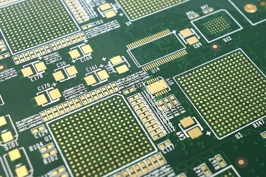
6 Layer PCB Manufacturing Capabilities
At JHYPCB, we are equipped with advanced multilayer PCB manufacturing lines specifically optimized for 6 layer board production.
Our process capabilities cover a wide range of materials, stackup configurations, copper weights and surface finishes to meet the most demanding design requirements from OEMs worldwide.
6 Layer PCB Fabrication Specifications
| Specification | JHYPCB Capability |
|---|---|
| Number of Layers | 6 |
| Board Thickness | 0.8mm – 3.2mm (standard 1.6mm) |
| Copper Weight (Outer) | 0.5 oz – 4 oz |
| Copper Weight (Inner) | 0.5 oz – 2 oz |
| Minimum Line Width / Spacing | 3/3 mil |
| Minimum Mechanical Drill | 0.2mm |
| Minimum Laser Drill (HDI) | 0.1mm |
| Board Size | Max 600mm × 600mm |
| Surface Finish | HASL, Lead-free HASL, ENIG, OSP, Immersion Silver, Immersion Tin, ENEPIG |
| Solder Mask Color | Green, Black, White, Blue, Red, Yellow, Purple |
| Controlled Impedance | ±5% / ±10% tolerance |
| Blind & Buried Vias | Supported |
| Via-in-Pad | Supported |
| IPC Standard | IPC-Class 2 (default) / IPC-Class 3 (available) |
| Material Options | FR4 (Tg 135 / 150 / 170), High-Speed FR4, Rogers, Halogen-Free |
| Maximum Aspect Ratio | 10:1 |
| Bow & Twist | ≤ 0.75% |
| Lead Time (Prototype) | As fast as 3–5 business days |
| Lead Time (Small Batch) | 7–15 business days |
6 Layer PCB Material Options
Choosing the right base material is critical for 6 layer PCB performance and reliability.
JHYPCB supports a full range of materials to match your electrical, thermal and mechanical requirements:
- Standard FR4 (Tg 135°C) – Cost-effective option for general-purpose digital and mixed-signal designs.
- Mid-Tg FR4 (Tg 150°C) – Better thermal stability for products subject to higher operating temperatures or lead-free soldering processes.
- High-Tg FR4 (Tg 170°C) – Recommended for industrial, automotive and high-reliability applications.
- High-Speed / Low-Loss FR4 – Optimized Dk/Df values for high-speed digital and signal integrity-critical designs (e.g., Isola, Shengyi S1000-2M).
- Rogers Series (RO4003C, RO4350B, RO3003 etc.) – Ideal for RF, microwave and mmWave designs requiring stable Dk across frequency and temperature.
- Halogen-Free FR4 – Meets RoHS and environmental compliance requirements for EU and North American markets.
Quality Assurance for Every 6 Layer PCB Order
- 100% Electrical Testing (Flying Probe or Fixture) – Every board is tested for opens and shorts before shipment.
- Automated Optical Inspection (AOI) – All inner and outer layers are inspected after etching and lamination.
- Impedance Control & Verification – Controlled impedance boards are tested with a TDR instrument and a test coupon report is provided.
- Cross-Section Analysis – Available upon request to verify hole wall quality, lamination integrity and copper thickness.
- IPC-A-600 Visual Inspection – Boards are visually inspected to IPC-Class 2 or Class 3 standards per customer requirements.
- UL, ISO 9001, IATF 16949 Certified – Manufacturing processes comply with internationally recognized quality management standards.
6 Layer PCB Design
6 Layer PCB Design Guidelines & DFM Support
A well-designed 6 layer PCB stackup and layout are the foundation of a manufacturable, reliable and high-performing board.
JHYPCB’s engineering team provides free Design for Manufacturability (DFM) review and stackup consultation for every order, helping customers avoid costly redesigns and production delays before fabrication begins.
Learn more about 4 Solutions to Reduce EMC in 6-layer PCB Design
Stackup Design Guidelines for 6 Layer PCBs
- Use a symmetrical stackup – Always design your 6 layer stackup symmetrically about the center to prevent board warping during lamination and reflow soldering.
- Pair every signal layer with a reference plane – Place each high-speed or critical signal layer adjacent to a ground or power plane to ensure short return paths and minimize loop inductance.
- Separate analog and digital ground zones – If your design mixes analog and digital signals, use dedicated inner plane areas or stitching vias to isolate return currents and reduce noise coupling.
- Use inner layers for sensitive high-speed routing – Routing critical signals on inner layers (sandwiched between reference planes) provides natural shielding and better EMI/EMC performance.
- Avoid routing signals on the same layer in both X and Y directions – Assign a preferred routing direction per layer (e.g., Layer 1 horizontal, Layer 3 vertical) to reduce interlayer crosstalk.
Controlled Impedance Design for 6 Layer PCBs
- Define your target impedance early – Specify target impedance values (typically 50Ω single-ended or 100Ω differential) on your stackup drawing or fabrication notes before submitting Gerber files.
- Calculate trace width based on your stackup – Impedance-controlled trace widths depend on copper weight, dielectric thickness and material Dk value; JHYPCB’s engineers can calculate and confirm these for you.
- Use dedicated test coupons – For IPC-compliant impedance verification, JHYPCB adds test coupons to the panel edges and provides a TDR measurement report for controlled impedance orders.
- Tolerance options available – Standard ±10% impedance tolerance is included; tighter ±5% tolerance is available upon request for RF and high-speed designs.
Routing & Via Design Recommendations
- Minimize via stubs – For high-speed signals above 3 GHz, consider back-drilling or blind vias to eliminate stub resonance effects that degrade signal quality.
- Use teardrops at via pads – Teardrops improve mechanical reliability and reduce the risk of via barrel cracking during thermal cycling.
- Maintain adequate via-to-trace clearance – Keep at least 6 mil (0.15mm) clearance between vias and adjacent traces on inner layers to avoid etching issues.
- Avoid placing vias directly under BGA pads unless via-in-pad filling and plating is specified – JHYPCB supports via-in-pad with copper or resin fill for high-density BGA designs.
- Use differential pair routing rules – Keep differential pairs tightly coupled, maintain matched lengths and route through the same layer where possible to preserve timing and impedance balance.
Thermal & Mechanical Design Considerations
- Select the right Tg material for your operating environment – Use High-Tg FR4 (Tg 170°C) or better for boards subject to lead-free soldering, high ambient temperatures or automotive operating conditions.
- Add thermal relief to inner plane connections – Thermal relief spokes on inner power and ground plane connections improve solderability during wave or reflow soldering.
- Plan for mechanical stress at board edges and mounting holes – Keep traces and vias at least 0.3mm away from board edges, and add adequate annular rings around mounting holes to prevent cracking.
- Consider bow and twist in large panels – For boards larger than 300mm in any dimension, discuss panelization and fiducial placement with JHYPCB’s engineers to minimize warpage.
Free DFM Review – Submit Your Files Before You Order
Not sure if your 6 layer PCB design is fully optimized for manufacturing?
JHYPCB offers a free, no-obligation DFM review for all new inquiries.
Simply upload your Gerber files and stackup notes, and our engineering team will check for potential issues including drill-to-copper spacing, annular ring size, impedance stack-up consistency, copper balance and more — typically within 24 hours.
6 Layer PCB Cost & Lead Time
Understanding the cost drivers and lead time options for 6 layer PCB fabrication helps you plan your project budget and timeline more effectively.
At JHYPCB, we offer transparent pricing with no hidden fees, flexible lead time options from quick-turn prototype to volume production, and dedicated account support for customers in North America and Europe.Lorem ipsum dolor sit amet, consectetur adipiscing elit. Ut elit tellus, luctus nec ullamcorper mattis, pulvinar dapibus leo.
Key Factors That Affect 6 Layer PCB Cost
01
Board Size & Quantity
Larger boards and higher quantities reduce the unit cost significantly. Prototype pricing is higher per unit but has no minimum order quantity (MOQ) requirement at JHYPCB.
02
Base Material
Standard FR4 is the most cost-effective option. High-Speed FR4, Rogers or specialty laminates carry a material premium depending on the grade selected.
03
Copper Weight
Heavier copper (2 oz and above) requires more etching time and material, increasing fabrication cost compared to standard 1 oz copper weight.
04
Board Thickness & Stackup Complexity
Non-standard thicknesses, very thin boards (under 1.0mm) and asymmetric stackups may increase cost due to additional process controls required.
05
Surface Finish
HASL is the most economical option. ENIG, ENEPIG and Immersion Silver carry a slight premium but offer better flatness, shelf life and solderability for fine-pitch components.
06
Controlled Impedance
Impedance-controlled orders require additional engineering review, test coupon fabrication and TDR verification, which adds a modest cost increment.
07
Blind & Buried Vias / Via-in-Pad
HDI features such as blind vias, buried vias and filled via-in-pad significantly increase process complexity and fabrication cost compared to standard through-hole vias.
08
Special Requirements
Edge plating, gold fingers, countersinks, controlled depth routing (back-drilling) and other special features each carry additional processing charges.
6 Layer PCB Lead Time Options
| Quick-Turn Prototype | Small Batch | Medium to Large Batch | |
|---|---|---|---|
| Typical Quantity | 1 – 10 pcs | 10 – 200 pcs | 200+ pcs |
| Standard Lead Time | 5 – 7 business days | 7 – 12 business days | 12 – 20 business days |
| Expedited Option | As fast as 3 business days | As fast as 5 business days | Available upon request |
| Impedance Control | Available | Available | Available |
| DFM Review | Included (free) | Included (free) | Included (free) |
| Engineering Support | Included | Included | Dedicated account manager |
Note: Lead times are counted from the date of Gerber file confirmation and full payment. International shipping time to North America and Europe is typically 3–7 business days via DHL, FedEx or UPS.

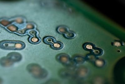
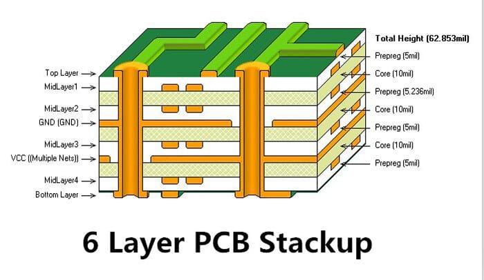
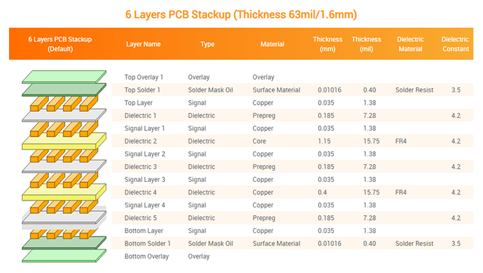
Fig.9
6 Layer PCB Fabrication – Drilling
How to Get an Accurate 6 Layer PCB Quote from JHYPCB
The fastest way to receive a precise quote is to submit your Gerber files along with a completed stackup specification, including board dimensions, layer count, copper weight, surface finish, quantity and any special requirements such as controlled impedance or blind vias.
Our sales and engineering team typically responds within 2–4 business hours during working days.
Step 1
Submit Files
Upload your Gerber files, BOM (if PCBA) and stackup notes via our online quote form or email.
Step 2
Engineering Review & Quote
Our team reviews your files, performs a free DFM check and sends back a detailed quotation within 2–4 business hours.
Step 3
Confirm & Production Starts
Once you approve the quote and confirm payment, production is scheduled immediately with real-time order tracking available.
Ready to get a competitive price for your 6 layer PCB?
Submit your Gerber files now and receive a detailed quote within 4 business hours — no commitment required.
Why Choose JHYPCB as Your 6 Layer PCB Manufacturer
With hundreds of global OEM customers relying on JHYPCB for multilayer PCB fabrication, we have built our reputation on engineering expertise, process consistency and honest communication — not just competitive pricing.
Here is what sets JHYPCB apart as a trusted 6 layer PCB manufacturing partner for customers in North America, Europe and beyond.
What Makes JHYPCB Different
Advanced Multilayer Fabrication Capability
Our production lines are fully equipped for 6 layer and above multilayer PCB manufacturing, supporting fine lines down to 3/3 mil, laser-drilled microvias, blind & buried vias, via-in-pad and controlled impedance with TDR verification — all under one roof.
Engineering-First Approach
Every order is reviewed by our in-house engineering team before production starts. We proactively flag DFM issues, suggest stackup optimizations and confirm impedance targets with customers — preventing costly delays and respins before they happen.
Strict Quality Management System
JHYPCB operates under ISO 9001-certified quality management processes. Every 6 layer PCB order goes through AOI on inner and outer layers, 100% electrical testing (flying probe or fixture), impedance coupon testing and IPC-A-600 visual inspection before shipment.
Transparent Pricing & No Hidden Fees
We provide itemized quotations covering all tooling, engineering, testing and packaging charges upfront. There are no surprise fees at invoicing — what you see in the quote is what you pay.
Reliable Global Logistics
We ship to North America and Europe via DHL, FedEx and UPS Express with full tracking and commercial invoice documentation included. Our team handles export compliance to ensure smooth customs clearance for customers in the US, Canada, UK and EU member states.
One-Stop PCB & PCBA Services
Beyond bare board fabrication, JHYPCB offers full turnkey PCB assembly (PCBA) including SMT, through-hole, BGA rework, functional testing and box-build — giving you a single, accountable supplier from design to finished product.
Certifications & Quality Credentials
JHYPCB’s manufacturing and quality systems are certified and audited to internationally recognized standards, giving our global customers confidence in every shipment:
- ISO 9001:2015 – Quality Management System certification
- UL Certification – UL-listed PCB manufacturer
- RoHS & REACH Compliant – All materials and processes comply with EU RoHS and REACH environmental regulations
- IPC Member – Manufacturing processes aligned with IPC-A-600, IPC-6012 and IPC-2221 standards
- IATF 16949 – Automotive-grade quality management capability for automotive electronics customers
What Our Customers Say
Get your free quote and DFM review today.
Partner with a 6 layer PCB manufacturer that treats every order — prototype or production — with the same engineering rigor and quality commitment.
Frequently Asked Questions About 6 Layer PCB Manufacturing
Have questions about 6 layer PCB design, stackup, cost or ordering process? We have compiled the most common questions from our global customers below. If you do not find the answer you need, feel free to contact our engineering team directly.
A 6 layer PCB is a multilayer printed circuit board with six copper layers separated by insulating dielectric material. You should consider a 6 layer design when your project requires higher routing density than a 4 layer board can provide, needs controlled impedance for high-speed signals, requires dedicated internal power and ground planes for better power integrity, or must meet strict EMI/EMC performance requirements.
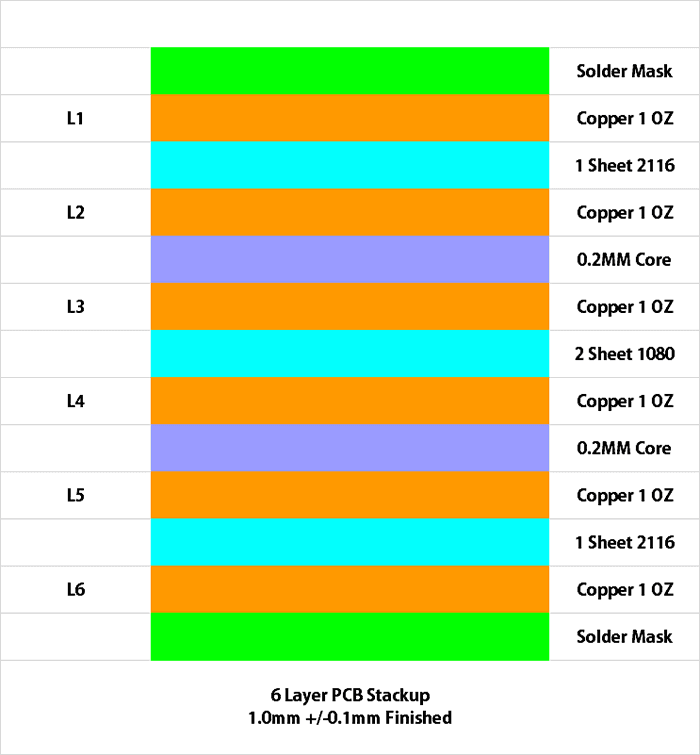
The most common standard thickness for a 6 layer PCB is 1.6mm. JHYPCB supports a wide range from 0.8mm to 3.2mm to accommodate space-constrained or ruggedized designs.
The most widely used 6 layer PCB stackup is: Top Signal – Ground – Inner Signal – Power – Ground – Bottom Signal. JHYPCB's engineering team can recommend and confirm the best stackup for your specific design at no charge.
Yes. JHYPCB supports standard ±10% and tighter ±5% impedance tolerance, with TDR measurement reports provided for all controlled impedance orders.
There is no minimum order quantity. We accept orders from a single piece upward, with volume pricing available for 10 pieces and above.
Prototype lead time is 5–7 business days, with expedited quick-turn available in as little as 3 business days. Small batch production typically takes 7–12 business days.
JHYPCB accepts Gerber RS-274X (preferred), ODB++ and IPC-2581, along with drill files, stackup notes and fabrication drawings.
Yes. Blind vias, buried vias and via-in-pad (copper or resin fill) are all supported for HDI 6 layer designs.
Yes. Rogers RO4003C, RO4350B, RO3003 and selected Isola/Shengyi high-speed materials are supported. Hybrid Rogers + FR4 stackups are also available.
Yes. Full turnkey PCBA including SMT, BGA, AOI, X-ray inspection and functional testing is available alongside bare board fabrication.
Still have questions about your 6 layer PCB project? Our engineering team is ready to help.


