Table of Contents
Introduction
In today’s fast-paced electronics world, high-speed circuits are everywhere—from USB 3.2 interfaces and PCIe Gen5 lanes to 10G Ethernet switches and DDR5 memory modules. As data rates climb beyond 5 Gbps, signal integrity becomes non-negotiable, and a well-designed 6-layer PCB is often the perfect solution for balancing performance, density, and cost.
Why choose a 6-layer board over simpler 4-layer designs? A dedicated stackup with multiple ground planes, power distribution layers, and separated signal routing minimizes crosstalk, reflections, and EMI while providing the routing channels needed for complex high-I/O devices like BGAs with fine-pitch balls. Unlike 4-layer boards, which struggle with return path continuity at gigabit speeds, 6 layers offer flexibility for impedance-controlled traces and efficient power delivery—ideal for mixed-signal, high-power, or RF-adjacent applications.
This complete guide walks you through designing a 6-layer PCB for high-speed circuits step by step. We’ll cover optimal stackups (building on our 6 Layer PCB Stackup Design Guide), impedance control techniques, routing strategies, power integrity tips, and manufacturing considerations. Whether you’re an engineer tackling your first high-speed prototype or optimizing for production, these proven practices will help you achieve reliable signal integrity and pass EMC compliance on the first spin. Let’s dive in.
6 Layer PCB Stackup for High-Speed Signals
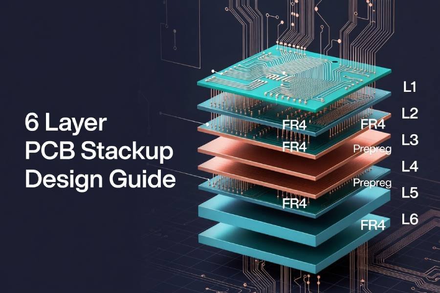
The foundation of any high-speed 6-layer PCB design starts with the stackup—the precise arrangement of copper layers, dielectrics, and planes that determines signal quality, impedance, and EMI performance. For speeds above 1 GHz (think USB 3.2 at 10 Gbps or PCIe Gen4), poor stackup choices lead to crosstalk, ground bounce, and signal degradation, often requiring costly respins.
Recommended 6-Layer Stackup Configurations
Here are three proven stackups tailored for high-speed signals, based on industry standards from Altium, Cadence, and fab houses like JLCPCB. Each prioritizes adjacent ground planes for return paths and symmetric construction to prevent warping.
| Stackup Type | Layer 1 | Layer 2 | Layer 3 | Layer 4 | Layer 5 | Layer 6 | Best For |
|---|---|---|---|---|---|---|---|
| Symmetric High-Speed (Most Common) | Top Signal (High-Speed) | Ground | Power | Inner Signal (Diff Pairs) | Ground | Bottom Signal | USB, PCIe, Ethernet; balanced EMI performance |
| EMI-Optimized | Signal | Ground | Power | Core Gap / Inner Signal | Signal | Ground | Noisy environments; improved shielding |
| Power-Heavy | Top Signal | Ground | Power 1 | Power 2 / Ground | Ground | Bottom Signal | High-current and power-dense applications |
Pro Tip: Use the symmetric stackup for most designs—Layer 1 and 6 for components/high-speed outer traces, Layers 3/4 for dense inner routing. Prepreg/core thicknesses: Aim for 0.1-0.2 mm between signal/ground for 50Ω impedance.
Key Stackup Design Principles for High-Speed
- Reference Planes: Every high-speed signal layer needs an adjacent ground plane (within 5-10 mils) for low-inductance return paths, reducing loop area and EMI. Avoid splitting grounds under signals.
- Dielectric Symmetry: Match core/prepreg thicknesses top-to-bottom to minimize bow/warp—critical for BGA assembly.
- Thermal Management: Intersperse power planes for heat spreading; thicker copper (2 oz) on inner PWR layers for high-current paths.
- Thickness Impact: Reference our 6 Layer PCB Thickness Guide for standard 1.6 mm boards—thinner stacks (<1.0 mm) excel in high-frequency but raise impedance challenges.

The stackup above illustrates a symmetric 6-layer example with glowing high-speed traces on outer layers and solid ground/power planes for shielding. Simulate your stackup early in tools like Polar SI9000 or Altium’s Layer Stack Manager to verify impedance before routing. With the right stackup, your high-speed signals will fly clean.
Impedance Control in 6 Layer High-Speed PCBs
Impedance control is critical in 6-layer high-speed PCBs because it helps prevent signal reflections that can distort waveforms at gigabit data rates. Without proper impedance matching, differences between the transmission line and the driver/receiver interface can cause overshoot, ringing, and data errors, especially in interfaces such as PCIe, USB, and other high-speed serial buses.
In a 6-layer PCB stackup, controlled impedance makes signal behavior more predictable and helps maintain signal integrity across different routing layers. It also supports more stable propagation delay, lower return loss, and better overall high-speed performance.
Understanding Characteristic Impedance
Characteristic impedance, usually written as \( Z_0 \), is the ratio of voltage to current along a transmission line. In high-speed PCB design, the most common targets are 50Ω for single-ended traces and 100Ω for differential pairs.
The actual impedance depends on several physical factors, including trace width, copper thickness, dielectric constant, and the distance between the signal trace and its reference plane.
This formula is commonly used when the trace is routed on an outer layer and referenced to a nearby plane.
This expression is typically used for inner-layer traces that are fully surrounded by dielectric material and reference planes.
In these formulas, \( w \) is the trace width, \( h \) is the height from the trace to the reference plane, \( t \) is the copper thickness, \( b \) is the spacing between reference planes in a stripline structure, and \( \epsilon_r \) is the dielectric constant of the material.
Microstrip vs. Stripline in 6-Layer Boards
| Type | Location | Advantages | Limitations | Typical Use |
|---|---|---|---|---|
| Microstrip | L1 / L6 (outer layers) | Easier to fabricate and inspect; wider trace widths | Higher radiation and EMI sensitivity | Shorter high-speed runs, USB, general routing |
| Stripline | Inner signal layers | Better shielding and more stable impedance | Narrower traces and tighter fabrication tolerance | Longer high-speed routes, PCIe, DDR, dense designs |
For example, a 50Ω microstrip on a typical 1.6 mm 6-layer board may require a trace width in the range of about 5 to 7 mil, depending on the exact dielectric thickness and material properties. A 100Ω differential pair will also depend heavily on pair spacing and stackup geometry.
How to Achieve and Verify Controlled Impedance
- Define impedance targets early. Decide whether the design requires 50Ω single-ended, 90Ω differential, 100Ω differential, or other interface-specific values before routing begins.
- Work with the PCB manufacturer. Confirm the real stackup, dielectric data, copper thickness, and fabrication tolerance before finalizing trace widths.
- Use impedance calculators or field solvers. Tools such as Polar SI9000, Saturn PCB Toolkit, or your EDA stackup manager can help predict the actual geometry needed.
- Request impedance testing. TDR coupon testing is commonly used by PCB manufacturers to verify whether the fabricated board meets the target impedance range.
In most practical designs, impedance control should not be treated as a routing-only topic. It is closely tied to stackup planning, material selection, fabrication capability, and signal integrity requirements. The earlier it is considered in the design flow, the more reliable the final 6-layer high-speed PCB will be.
Routing Strategies for High-Speed Traces
With your 6-layer stackup and impedance specs locked in, routing high-speed traces demands precision to preserve signal quality. Poor routing introduces skew, crosstalk, and EMI, turning clean eye diagrams into noise. In 6-layer boards, leverage inner layers for dense signals while keeping outer layers for critical nets adjacent to ground planes.
Core Routing Guidelines for 6-Layer High-Speed PCBs
Follow these rules to route traces like a pro:
- Reference Plane Continuity: Route over unbroken ground planes (L2/L5); use stitching vias every 1/20 wavelength (e.g., 3-5 mm at 5 GHz).
- Min Trace/Via Specs: High-speed: 4-6 mil width, 5 mil spacing; vias <10 mil drill for <1% insertion loss.
- Orthogonal Routing: 90° angles between layers (L1 horizontal, L4 vertical) to cut crosstalk by 20 dB.
Differential Pair Routing Mastery
Differential pairs (USB, PCIe, LVDS) are high-speed staples—route them as symmetric twins for common-mode rejection.
| Guideline | Rule | Why It Matters |
|---|---|---|
| Length Matching | Intra-pair skew <5-10 mils (±0.127-0.254 mm) | Prevents phase shift, eye closure |
| Spacing Consistency | Fixed gap (6-8 mil for 100Ω); no bends >45° | Maintains Z_diff ±10% |
| Layer Preference | Same layer; via together if changing | Uniform propagation |
Serpentine for Skew Fix: Extend shorter trace with smooth meanders (amplitude 3x width, spacing >2x gap). Tools like Altium auto-tune.
Via Optimization & Advanced Techniques
Vias are impedance bumps—minimize them:
- Via-in-Pad or Blind/Buried: For BGAs; backdrill stubs >1/10 wavelength.
- Length Tuning: Fanout DDR clocks with <5 ps skew using trombone patterns.
- Broadside Pairs: Adjacent layers for density (L1/L4), tight coupling.
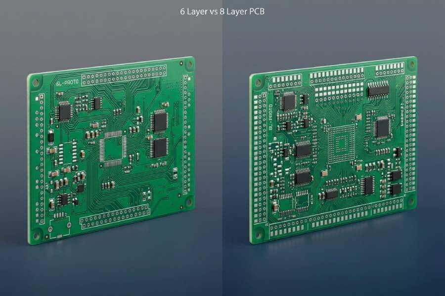
Pro Tip: Link to our 4 Layer vs 6 Layer PCB guide for routing density comparisons—6 layers give 2x channels without chaos. Route iteratively: High-speed first, verify with HyperLynx sim. Solid routing sets up power integrity next.
Power Integrity and Ground Planes in 6 Layer Design
Power integrity (PI) ensures stable voltage delivery to high-speed ICs despite transient currents from simultaneous switching. In 6-layer PCBs, dedicated power (PWR) and ground (GND) planes form the backbone of the Power Distribution Network (PDN), targeting <10 mΩ impedance up to 1 GHz. Weak PI causes voltage droop, jitter, and false clocks—fatal for PCIe or DDR4/5.
Optimizing Planes in 6-Layer Stackups
Position PWR/GND planes strategically: Adjacent pairs (e.g., L3 PWR next to L2/L4 GND) create distributed capacitance (~1 nF/cm²), filtering noise.
Best Practices Table:
| Aspect | Guideline | Benefit |
|---|---|---|
| Ground Planes | Solid pours on L2/L5; stitch splits with vias (grid λ/20) | Low-inductance returns; EMI shield |
| Power Planes | L3/L4 for multi-rails; no splits under signals | Low PDN impedance; <50 mV droop |
| Coupling | PWR-GND spacing <10 mil | Higher decoupling capacitance |
| Splitting | Domain splits >50 mil from signals; fence vias | Isolate noisy rails |
Symmetric Rule: Mirror PWR/GND top-bottom for warp-free boards.
Decoupling Capacitor Strategies
Decaps bridge PDN impedance peaks—place them right:
- Tiered Approach: 0.1 µF ceramic (<1 mm from pins) for >100 MHz; 10-100 µF bulk for low-freq.
- Placement: Underneath BGA/IC; via <5 mil to plane. Target 4-16 decaps per power pin.
- Value Selection: ESR <0.1 Ω; simulate target impedance curve (SIwave/Ansys).
Example PDN Target: <1 mΩ DC to 100 MHz, peaking at 500 MHz—decaps fill gaps.
Reference our 6 Layer vs 8 Layer comparison for scaling PI to more layers. Solid PI feeds clean signals—next, signal integrity simulations seal the deal.
Signal Integrity Best Practices
Signal integrity (SI) ensures high-speed signals arrive undistorted despite losses, noise, and interactions. In 6-layer PCBs, combining stackup, impedance, and routing yields open eye diagrams (>80% height/width)—critical for BER <10^-12 in PCIe or Ethernet. Violations cause data errors, EMI failures, or redesigns.
Controlling Crosstalk, Reflections, and Attenuation
Crosstalk: Capacitive/inductive coupling between traces.
| Issue | Cause | Mitigation |
|---|---|---|
| Near-End Far-End | Parallel runs >3x rise time | >3w spacing; guard traces; orthogonal layers |
| Aggressor/Victim | <10 mil gap | Increase separation; ground fill stitching |
Reflections: Impedance discontinuities (vias, bends).
- Series termination (22-33Ω) for source; parallel for receiver.
- Backdrill vias; <45° mitered corners.
Attenuation: Dielectric/conductor loss at >5 GHz.
- Shorter traces; low-loss FR4 (Dk<4.0); wider traces.
EMI/EMC Solutions for 6 Layers
Leverage planes for shielding:
Stitch GND edges (λ/20 vias).
Separate analog/digital; ferrite beads on noisy nets.
Link to our .
Simulation and Eye Diagram Analysis
Pre/post-layout SI tools predict issues:
HyperLynx/SIwave: IBIS models for eye sims (aim 200 mV height, 0.7 UI width).
Keysight ADS: Channel sim with S-parameters.
Eye Diagram Metrics:
Height: Logic swing margin.
Width: Timing jitter tolerance.
Jitter: <10% UI.
Verify with oscilloscope post-fab. These practices, layered on PI, make your 6-layer board bulletproof for manufacturing.
6 Layer High-Speed PCB Manufacturing Considerations
Transitioning from design to fabrication for high-speed 6-layer PCBs requires tight tolerances to preserve impedance, minimize loss, and ensure reliability. Poor manufacturing turns a great design into a dud—focus on fab capabilities, materials, and DFM. PCBELEC specializes in prototypes with ±10% impedance control and quick turns.
Material Selection for High-Speed Performance
FR4 dominates cost-sensitive designs, but high-speed demands low-loss variants:
| Material | Dk/Df @1GHz | Cost | Best For |
|---|---|---|---|
| Standard FR4 (TG135) | 4.4/0.02 | $$ | <5 Gbps USB/Ethernet |
| High-TG FR4 (TG170) | 4.2/0.015 | $$$ | DDR4, up to 10 Gbps |
| Rogers RO4003C | 3.38/0.0027 | $$$$$ | RF/10G+; low loss |
| Hybrid (FR4+Rogers) | Mixed | $$$$ | Cost-effective high-freq |
Tip: FR4 suffices for most <10 Gbps; Rogers for radar/5G. Specify Df <0.01 for >5 GHz. Reference our for stackup-compatible cores.
Key Manufacturing Specs & Cost Factors
Expect 30-50% premium over 4-layer due to lamination complexity.
| Factor | Spec for High-Speed | Impact |
|---|---|---|
| Copper Weight | 1/2-2 oz inner; ±5% etch | Thicker for PI |
| Drill/Via Tolerance | ±0.05 mm; backdrill stubs | Low loss |
| Impedance Test | TDR coupons; ±10% | SI guarantee |
| Solder Mask | LPI; 0.3 mil clearance | Trace protection |
| Cost Drivers | Layer count, blind vias, volume | Prototypes $200-500/5 pcs |
DFM Checklist:
- Min annular ring 4 mil; no acute angles.
- Panelize for prototypes; IPC Class 2/3.
- Cost link: See our 6 Layer Cost Breakdown.
Choose fabs like PCBELEC for high-speed expertise—tight registration ensures alignment. With fab in mind, your design yields first-pass success.
Conclusion & Next Steps
Mastering 6-layer PCB design for high-speed circuits boils down to integrated choices: symmetric stackups with ground shielding, precise impedance control (±10%), careful differential routing with length matching, robust PDN/decoupling, SI verification via eye diagrams, and high-speed materials like low-loss FR4.
Key Takeaways Checklist:
- Stackup: Signal-GND-PWR-Signal-GND-Signal for optimal returns.
- Impedance: Microstrip/stripline calcs; TDR fab test.
- Routing: Skew <10 mils; stitching vias.
- PI/SI: Decaps near pins; sim before fab.
- Fab: ±10% Z control; reference DFM guides.
Ready to build? Start with our free stackup review service—upload your Gerber files for impedance/DFM feedback. Get instant quotes for high-speed 6-layer prototypes at PCBELEC, with delivery in 7-10 days.
Contact us today for your high-speed project—let’s make your signals fly!