Table of Contents
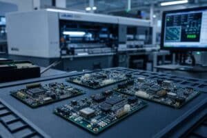
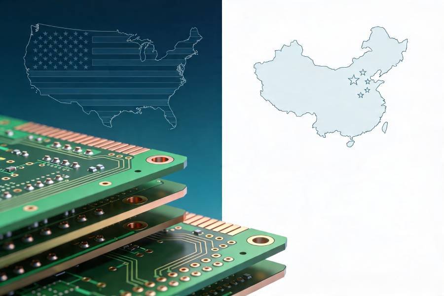
Choosing a multilayer PCB manufacturer is no longer as simple as picking the closest shop on a map. For high‑density designs, high‑speed signals, and tight launch schedules, the wrong partner can mean delayed projects, repeated respins, and unexpected cost overruns. At the same time, the global PCB supply chain has never been more diverse: you can work with large, established manufacturers in the United States, or you can tap into cost‑effective specialists in China that build multilayer boards every day for international customers.
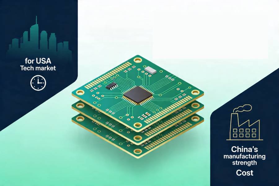
If you have ever searched for “best multilayer PCB manufacturers in the United States” or “multilayer PCB fabrication services near me,” you have probably noticed the same issue: there are many names on the market, but very little guidance on how to tell which one is actually a good fit for your project. This article cuts through the noise by first outlining what really defines a “best” multilayer PCB manufacturer in the U.S., then highlighting well‑known American companies, and finally showing when it makes sense to consider a cost‑effective China alternative like JHYPCB.
Whether you are building a four‑layer prototype for a startup product or a complex high‑layer‑count board for industrial or telecom applications, the goal is the same: find a reliable partner that can hit your performance, quality, and budget targets—without slowing your team down.
What Makes a “Best” Multilayer PCB Manufacturer in the U.S.?
Before looking at specific company names, it is worth asking a simple question: what does “best” actually mean in the context of multilayer PCB manufacturing? For some engineers, it means the ability to handle very high layer counts and exotic materials; for others, it means fast, affordable prototypes with strong engineering support. In practice, the best multilayer PCB manufacturer for your project is the one that aligns with your technical requirements, risk profile, and total cost expectations.
Below are the key criteria that experienced OEMs and hardware teams use when evaluating multilayer PCB manufacturers in the United States.
Technical Capabilities and Layer Count
The first and most obvious filter is technical capability. A manufacturer that primarily builds simple two‑layer boards is unlikely to be a strong partner for dense multilayer designs. When you review potential suppliers, look for:
- Supported layer counts (for example: 4–10 layers for mainstream applications, 12+ layers for advanced telecom, networking, or computing designs).
- Experience with HDI, blind and buried vias, via‑in‑pad, and fine‑pitch BGA breakout.
- Typical minimum trace/space, hole sizes, and aspect ratios that the factory can reliably achieve.
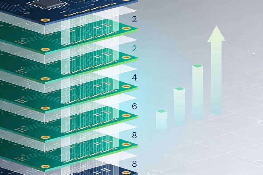
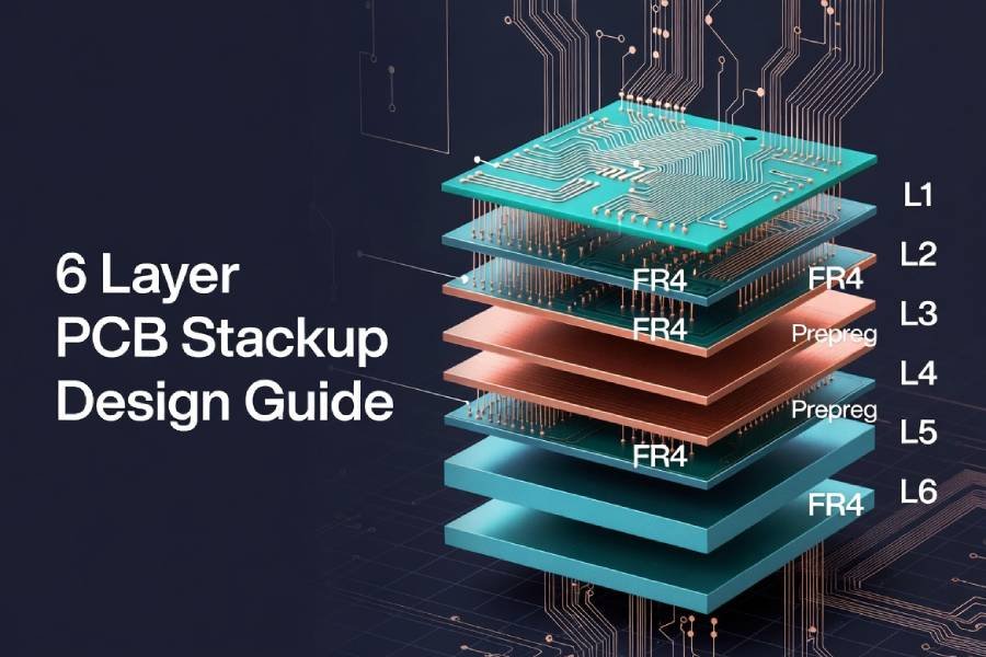
If your design involves controlled impedance or high‑speed signals, the ability to design and fabricate optimized stackups becomes even more important. In that case, you should verify whether the manufacturer provides stackup suggestions, simulation support, or at least reference stackup tables for common layer counts such as 4‑layer, 6‑layer, and 8‑layer boards.
Materials and Certification Readiness
A second key dimension is the manufacturer’s material portfolio and their readiness to meet industry‑specific standards. For example, many U.S. multilayer PCB manufacturers maintain strong expertise with:
- High‑Tg FR‑4 laminates for mainstream industrial and consumer electronics.
- High‑speed / low‑loss materials (such as advanced epoxy or PTFE‑based substrates) for telecom, networking, and RF applications.
- High‑temperature or high‑reliability materials for automotive, aerospace, and medical devices.
In regulated industries, certifications often matter as much as raw capability. Depending on your application, you may need suppliers that hold:
- ISO 9001 and ISO 13485 for quality and medical devices.
- AS9100 for aerospace and defense.
- UL recognition for specific laminates and flammability classes.
- ITAR compliance and secured facilities for defense‑related work in the United States.
If your project will eventually require regulatory approvals or customer audits, working with a multilayer PCB manufacturer that already meets these certification requirements can save months of qualification effort.
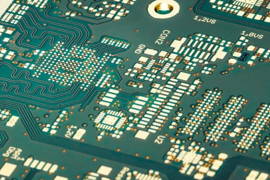
Quality, Yield, and Reliability
Even the most impressive capability list does not mean much if the factory cannot maintain stable quality and yield over time. For multilayer PCBs, inner‑layer registration, lamination quality, and plating uniformity all have a direct impact on reliability and field performance.
When you compare U.S. multilayer PCB manufacturers, ask about:
- Historical yield rates for similar stackups and layer counts.
- Standard electrical test coverage (flying probe vs fixture‑based testing).
- Inner‑layer inspection methods and AOI coverage.
- Process controls for lamination, drilling, and copper plating.
If a supplier can share representative quality metrics or case studies from projects similar to yours, that is usually a good sign that they understand how to manage multilayer complexity at scale.
Lead Time and Quick‑Turn Prototypes
For many engineering teams, lead time is just as important as per‑unit price. Prototype cycles are often measured in weeks, and every additional day of delay can push product launches and customer demos.
Most established U.S. multilayer PCB manufacturers offer several service tiers, such as:
- Standard lead time for cost‑optimized builds.
- Quick‑turn or express options for urgent prototypes.
- Dedicated prototype lines or small‑batch services for early‑stage designs.
When evaluating different suppliers, pay attention not only to the headline lead time but also to how realistic those numbers are for your stackup, materials, and layer count. A factory that can reliably deliver a six‑layer board in one week may be more valuable than one that promises three days but frequently slips schedules.
Learn more about our Quick Turn PCB Manufacturing services.
DFM Support and Engineering Communication
Multilayer designs are rarely perfect on the first try. A manufacturer that provides strong DFM (Design for Manufacturability) support and responsive engineering feedback can help you avoid costly respins before you even place an order.
Good signs include:
- Pre‑production engineering review of Gerber, ODB++ or IPC‑2581 data.
- Clear, constructive DFM reports that highlight potential issues with stackup, clearances, hole sizes, or impedance structures.
- Direct access to CAM or process engineers who can answer detailed questions.
For U.S.‑based manufacturers, time‑zone alignment and language familiarity can further speed up this feedback loop, which is particularly valuable when project timelines are tight.
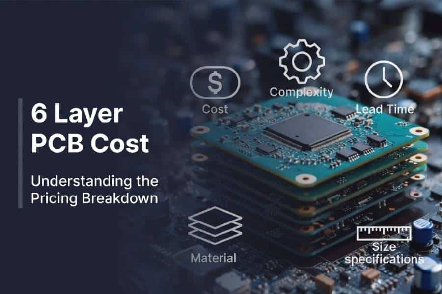
Total Cost and Supply Chain Stability
Finally, while cost is often the first metric people think about, for multilayer boards it should be viewed as part of a broader total cost of ownership picture. Higher per‑unit pricing from a U.S. manufacturer may still be justified if they help you avoid design mistakes, reduce field failures, or shorten time‑to‑market. On the other hand, many companies now balance local suppliers with cost‑effective partners in China to optimize different phases of the product lifecycle.
When comparing quotes from U.S. multilayer PCB manufacturers, consider:
- Engineering and setup charges for prototypes and small batches.
- Price scaling as you move from prototypes to volume.
- Shipping costs, logistics complexity, and buffer stock strategies.
Top Multilayer PCB Manufacturers in the United States
With the evaluation criteria in mind, it becomes much easier to look at specific companies and understand what they are actually good at. The U.S. PCB industry includes a wide mix of very large, global manufacturers and highly specialized regional shops. Below are some of the best‑known multilayer PCB manufacturers in the United States that are frequently mentioned in industry rankings and buyer guides.
Note: This list is not exhaustive, and inclusion here does not represent an endorsement over other qualified suppliers. Instead, it gives you a starting point for your own vendor shortlist and due diligence.
TTM Technologies
TTM Technologies is often cited as one of the largest PCB manufacturers in the United States, with a strong focus on advanced multilayer designs and high‑reliability applications. The company operates manufacturing facilities in North America, Asia, and Europe, and serves demanding markets such as aerospace, defense, automotive, and data communications.
From a multilayer perspective, TTM’s capabilities are extensive: they support conventional multilayer designs with high layer counts—reportedly up to 60+ layers in some product lines—as well as HDI structures with microvias, buried vias, and complex sequential lamination processes. Their material portfolio spans low‑loss and ultra‑low‑loss laminates, high‑temperature substrates, RF materials, and halogen‑free options, making them a strong fit for high‑speed digital, RF, and mission‑critical systems.
If your project requires ITAR compliance, advanced documentation, and long‑term supply for high‑reliability products, a large manufacturer like TTM is often on the shortlist for OEMs in defense, aerospace, and automotive sectors.
Sanmina Corporation
Sanmina is another prominent name in the U.S. electronics manufacturing landscape, offering both PCB fabrication and full PCB assembly and system‑level services. With dozens of facilities across the Americas, Europe, and Asia, Sanmina supports customers in telecom, networking, medical, industrial, and defense markets.
On the PCB side, Sanmina produces mid‑ to high‑layer‑count boards, rigid‑flex constructions, and HDI designs with capabilities such as controlled impedance, laser‑drilled microvias, and multiple sequential laminations. Their documented capabilities include multilayer boards up to around 28 layers in certain facilities, with fine line/space geometries and via‑in‑pad structures for dense designs.
Because Sanmina also operates extensive PCB assembly (PCBA) and SMT lines, some OEMs prefer them as a one‑stop partner—from multilayer bare board fabrication to fully assembled and tested products. This can be particularly attractive if you need a vertically integrated supplier with strong quality systems and global logistics support.
Advanced Circuits
Advanced Circuits is widely known in the U.S. market for its quick‑turn PCB services and its focus on serving a large base of engineering teams and OEM customers. According to multiple industry overviews, the company positions itself among the top PCB manufacturers in the United States and offers expanded capabilities beyond basic prototypes, including multilayer and special‑feature boards.
For multilayer projects, Advanced Circuits supports a range of layer counts and options such as laser‑drilled microvias, cavity PCBs, heavy copper, RF/microwave boards, and stackups reportedly up to around 40 layers in certain product lines. This combination of quick‑turn capability and advanced options makes them a common choice for engineers who need to move from early prototypes to more complex pre‑production builds without changing suppliers.
If your priority is domestic quick‑turn service with the option to scale into more advanced multilayer requirements, Advanced Circuits is often on the radar for U.S. hardware teams.
Sierra Circuits
Based in Silicon Valley, Sierra Circuits focuses heavily on quick‑turn, high‑complexity PCB fabrication and assembly, with a strong emphasis on high‑speed, HDI, and rigid‑flex designs. Their main facility is reported to be around 70,000 square feet and equipped with modern fabrication and SMT equipment tailored to demanding applications.
Sierra Circuits highlights the ability to deliver bare PCBs in as little as one day and turnkey PCB assembly in about five days for suitable designs, which is particularly appealing for time‑critical prototype cycles. The company also holds a broad set of certifications relevant to multilayer and high‑reliability work, including AS9100D, ISO 9001, ISO 13485, ITAR, and multiple IPC and UL qualifications.
For teams building high‑speed digital, RF, or rigid‑flex multilayer boards that need fast, engineering‑driven iteration in the U.S., Sierra Circuits is often considered a strong candidate.
Other Notable U.S. Multilayer PCB Manufacturers
Beyond these well‑known names, there are many other U.S. manufacturers that offer solid multilayer capabilities, often with a more specialized focus. Industry lists and buyer guides frequently mention companies such as:
- Epec Engineered Technologies – providing engineered PCB and cable solutions with a focus on custom multilayer designs and value‑added services.
- Rush PCB Inc. – a Silicon Valley–based supplier known for quick‑turn PCB fabrication and assembly, including multilayer boards for prototypes and small production runs.
- Macrofab and CircuitHub – platforms that combine PCB manufacturing, assembly, and online ordering interfaces, often used for prototypes and low‑to‑medium‑volume builds.
There are also niche manufacturers that concentrate on specific segments such as automotive, RF/microwave, or rigid‑flex PCBs, and they can be excellent partners if your product requirements align with their core strengths.
How to Use This List in Your Vendor Selection Process
While it may be tempting to simply pick a name from a “top PCB manufacturers in the United States” list, the more effective approach is to treat these companies as starting points for a structured evaluation. For each potential supplier, you should:
- Map their strengths against your actual stackup, layer count, and material needs.
- Confirm certifications and compliance requirements relevant to your industry.
- Request example builds, DFM samples, or references from similar projects where possible.
- Compare realistic lead times and pricing across at least two or three vendors, not just headline marketing claims.
Pros and Cons of Choosing a U.S.-Based Multilayer PCB Manufacturer
Once you know who the major players are, the next step is to decide whether working with a U.S.-based multilayer PCB manufacturer actually makes sense for your specific project. For some applications, staying domestic is clearly the best choice; for others, a hybrid approach or a cost‑effective overseas partner will deliver better overall value.
Below are the main advantages and limitations you should consider when you look at multilayer PCB fabrication services in the United States.
Advantages of U.S.-Based Multilayer PCB Manufacturers
1. Strong Quality and Regulatory Compliance
One of the biggest perceived advantages of manufacturing multilayer PCBs in the United States is quality and regulatory alignment. Many American PCB manufacturers operate under strict quality systems such as ISO 9001, ISO 13485, and AS9100, and have deep experience with sectors that demand high reliability, including aerospace, medical, automotive, and industrial controls.
For projects that fall under ITAR or other export‑control regulations, using a U.S.-based manufacturer that is already registered and compliant can be a hard requirement rather than a preference. Keeping design data, Gerber files, and production within an ITAR‑compliant ecosystem significantly reduces legal risk and simplifies supply‑chain audits.
2. Faster and More Predictable Logistics
Domestic manufacturing also simplifies logistics. PCBs do not need to cross borders or wait in customs, which reduces transit time and avoids disruptions tied to geopolitical events, port congestion, or sudden changes in trade policy.
For many U.S. manufacturers, this translates into:
- Shorter and more predictable shipping times.
- Easier use of expedited freight when deadlines slip.
- Less time spent on import paperwork and customs clearance.
If your product roadmap is very time‑sensitive, the ability to make quick changes and get boards in a matter of days instead of weeks can be a decisive advantage.
3. Easier Communication and Collaboration
Working with a U.S.-based multilayer PCB manufacturer also makes real‑time collaboration more straightforward. Being in (or close to) the same time zone means engineering questions, DFM feedback, and urgent design changes can often be resolved in the same business day.
This is particularly valuable when:
- You are still iterating on the stackup or impedance structures.
- Your design requires multiple quick prototype spins.
- You need tight coordination between your PCB designer, signal integrity engineer, and the fabricator’s CAM team.
For on‑site audits or line qualifications, traveling to a domestic facility is also faster and less costly than visiting an overseas plant.
4. Stronger IP Protection and Data Security
Intellectual property protection is another frequently cited reason for keeping multilayer PCB manufacturing in the United States. Domestic manufacturers operate under U.S. law, which offers clear legal recourse in case of IP disputes and enforces stricter data‑handling and confidentiality requirements.
For highly proprietary designs—especially in defense, telecom infrastructure, or competitive consumer electronics—some companies prefer to keep both design data and production within a jurisdiction where they feel more confident about enforcement mechanisms.
Limitations and Trade‑Offs of Staying Only with U.S. Manufacturers
1. Higher Unit Costs and NRE Charges
The most obvious trade‑off of using U.S.-based multilayer PCB manufacturers is cost. Labor, overhead, and regulatory expenses in the United States are generally higher than in Asia, and this is reflected in PCB pricing—especially for complex multilayer or HDI designs.
Multiple cost comparisons show that:
- Per‑unit prices for equivalent boards can be significantly higher in the U.S. than at reputable factories in China, sometimes by 60–80% depending on volume and complexity.
- NRE (engineering and tooling) charges can also be higher, which impacts prototypes and small runs the most.
For startups, small teams, or cost‑sensitive products, this price gap can directly limit how many prototype iterations they can afford, or how aggressively they can price the final product.
2. Limited Cost Flexibility for High Layer Counts and Exotic Materials
As layer count, board size, and material complexity increase, the cost difference between U.S. and offshore production often becomes even more pronounced. High‑layer‑count stackups, sequential lamination, controlled impedance structures, and low‑loss materials all add process steps that are inherently labor‑ and equipment‑intensive.
Because many Chinese manufacturers spread these fixed costs over much larger production volumes, they can offer more competitive pricing for multilayer PCBs once processes are dialed in. In contrast, U.S. plants may have less flexibility to discount complex builds, particularly at low or medium volumes.
3. Capacity Constraints and Lead Time at Scale
While domestic logistics are simpler, U.S. PCB manufacturing capacity is not unlimited. In periods of high demand, certain plants may run close to full utilization, which can lengthen lead times for complex multilayer builds or large orders.
If your roadmap includes aggressive volume ramp‑up or you expect sudden spikes in demand, relying solely on domestic manufacturers may expose you to capacity bottlenecks and longer quoted lead times than you would see from large offshore factories that specialize in scale.
4. Fewer Low‑Cost Options for Early‑Stage Prototyping
For early‑stage projects where the design is likely to change several times, keeping costs down per prototype spin can be more valuable than optimizing for maximum logistics convenience. In this phase, paying premium U.S. rates for every iteration can quickly consume development budgets, especially if you are working with multilayer boards that already carry higher base costs.
This is one of the main reasons many hardware teams now use a hybrid sourcing strategy: they work with a U.S. manufacturer when local presence, certifications, or ITAR compliance is crucial, and complement that with cost‑effective multilayer PCB partners in China for less sensitive prototypes and commercial products.
When a U.S.-Based Manufacturer Is the Right Choice
In summary, U.S.-based multilayer PCB manufacturers are often the best fit when:
- Your project is in a regulated or mission‑critical industry that requires U.S. production and strict certifications (for example, aerospace, defense, or certain medical devices).
- You need very tight collaboration, frequent on‑site visits, or real‑time engineering interaction, and you want to minimize the friction of time zones and language.
- IP protection and legal jurisdiction are top priorities, and you prefer to keep all sensitive data and production inside the United States.
However, for many high‑layer‑count prototypes and cost‑sensitive commercial projects, it makes sense to at least compare U.S. quotes with a capable China‑based multilayer PCB manufacturer. In the next section, we will look at when a cost‑effective China alternative becomes the more attractive option—and why companies around the world increasingly rely on specialized partners like JHYPCB for multilayer PCB fabrication.
When a Cost-Effective China Alternative Makes Sense
As global supply chains have matured, China has become one of the world’s most important hubs for multilayer PCB fabrication. Many factories there specialize in high‑layer‑count boards and handle a large volume of international orders every day, which gives them considerable experience and economies of scale. For the right kind of project, working with a reputable China‑based multilayer PCB manufacturer can significantly reduce cost while still meeting demanding technical requirements.
Below are the situations where a cost‑effective China alternative is often worth serious consideration.
Lower Cost for Prototypes and Small- to Medium-Volume Builds
One of the most obvious advantages of manufacturing multilayer PCBs in China is cost. Due to lower labor costs, high production volumes, and optimized supply chains around copper‑clad laminates and chemicals, Chinese PCB manufacturers can typically offer more competitive pricing than U.S. factories for equivalent designs.
This difference is especially visible in:
- Early‑stage prototypes where engineering and tooling charges make up a large share of the total cost.
- Small‑ to medium‑volume orders that do not yet benefit from very large‑batch economies of scale in the United States.
- Complex multilayer boards where multiple lamination cycles and intricate processes amplify the baseline cost gap.
Lower per‑unit cost and NRE can allow your team to run more prototype iterations, experiment with alternative stackups, and refine your design before committing to a final version.
Strong Capabilities for High Layer Counts and Diverse Materials
China’s PCB industry has invested heavily in advanced multilayer and HDI capabilities. Many factories routinely build 4–12 layer boards for mainstream applications, and also support higher layer counts for telecom, networking, and industrial systems. It is common to find manufacturers offering:
- Sequential lamination and hybrid stackups.
- Blind and buried vias, microvias, and via‑in‑pad solutions.
- A wide range of materials from standard FR‑4 to high‑Tg and low‑loss laminates for high‑speed designs.
Because they serve a global customer base, these manufacturers often maintain up‑to‑date equipment and process controls comparable to those of leading Western factories. For many commercial and industrial applications that do not require ITAR or on‑shore production, this combination of capability and cost makes China a very attractive option.
Balanced Lead Times for International Projects
When a China-Based Partner Is a Good Fit
In practice, a cost‑effective China alternative is often the right choice when:
- Your product is commercial or industrial and does not fall under ITAR or strict local‑manufacturing mandates.
- You need to control BOM and PCB costs aggressively to maintain healthy margins, particularly for multilayer designs.
- You want to iterate quickly on prototypes without overspending on each revision.
- You are comfortable working with an experienced overseas supplier that has clear communication channels and a strong track record with international customers.
Many companies now adopt a dual‑sourcing strategy: they use U.S. manufacturers for sensitive or highly regulated programs, and partner with capable Chinese multilayer PCB suppliers for cost‑driven commercial products and high‑layer‑count prototypes.
Why JHYPCB Is a Strong China Alternative for Multilayer PCBs
Not all China‑based PCB manufacturers are the same. While the country has thousands of board houses, only a fraction of them combine advanced multilayer capabilities, export‑oriented quality systems, and the kind of responsive support that U.S. and European engineering teams expect. JHYPCB positions itself in this segment: as a focused multilayer PCB supplier that understands the needs of international customers building complex, time‑critical products.
Deep Experience in Multilayer PCB Fabrication
JHYPCB has built its core business around multilayer PCB fabrication rather than just simple two‑layer boards. The company manufactures a wide range of multilayer stackups for global customers, from standard 4‑layer and 6‑layer designs to higher layer counts used in industrial, telecom, and high‑performance applications.
Typical multilayer capabilities include:
- Support for standard and high‑Tg FR‑4 as well as higher‑performance materials for demanding designs.
- Controlled impedance stackups and tightly managed dielectric thicknesses.
- Blind and buried vias, via‑in‑pad structures, and sequential lamination processes for dense layouts.
- Fine line/space features suitable for modern digital and mixed‑signal boards.
Prototype-Friendly: Quick-Turn Multilayer PCB Services
One of the biggest reasons engineering teams look for a China alternative is the ability to run more prototype spins without destroying the budget. JHYPCB is deliberately set up to support quick‑turn multilayer PCB prototypes, not just large production orders.
For typical multilayer designs, JHYPCB can:
- Fabricate small‑batch 4‑layer and 6‑layer PCBs on accelerated schedules suitable for engineering builds.
- Offer competitive lead times for more complex stackups, while keeping pricing at a level that makes frequent revisions affordable.
- Combine prototype flexibility with production‑ready processes, so successful prototypes can transition into higher volumes with minimal re‑qualification.
This is particularly valuable when you are still refining your stackup, experimenting with different routing strategies, or tuning impedance and signal‑integrity performance. Instead of paying premium U.S. pricing for every spin, you can leverage JHYPCB to iterate quickly on multilayer designs while keeping overall development cost under control.
Quality Systems and Certifications for Global Customers
Cost‑effective does not mean cutting corners. JHYPCB operates with quality systems and process controls designed for long‑term cooperation with overseas customers. The company focuses on:
- Consistent layer‑to‑layer registration and lamination quality for multilayer boards.
- Comprehensive electrical testing (such as flying‑probe testing for prototypes and fixture‑based testing for volume orders) to verify connectivity.
- Visual inspection and AOI to catch fabrication defects before shipment.
- Traceable production records that help customers investigate any issues quickly if they arise.
Where applicable, JHYPCB also aligns with industry‑standard certifications and customer‑specific quality requirements, making it easier for U.S. and European teams to qualify the factory as an approved vendor.
Competitive Pricing Without Sacrificing Engineering Support
Because JHYPCB operates within China’s mature PCB supply chain, it can offer very competitive pricing on multilayer PCBs compared to typical U.S. manufacturing costs, especially for complex stackups and small‑ to medium‑volume orders. At the same time, the company invests in engineering support to keep communication clear and effective for international customers.
In practice, this means:
- Transparent quotations that break down material choices, surface finishes, and special processes for your multilayer design.
- DFM feedback to help you avoid manufacturability issues in your stackup and layout before you place a formal order.
- The ability to suggest cost‑optimized alternatives—such as standardizing on certain layer counts, thicknesses, or copper weights—without compromising performance.
For many teams, this combination of lower PCB cost and helpful engineering interaction directly translates into faster design cycles and fewer expensive respins.
A Service Model Tailored to U.S. and European Customers
Finally, JHYPCB has structured its service model with international customers in mind. The goal is to reduce friction compared to working with a purely domestic‑focused factory in China.
Key aspects include:
- English‑speaking sales and engineering contacts who can understand and respond to detailed technical questions.
- Familiarity with common design file formats (Gerber, ODB++, IPC‑2581) and documentation standards used by U.S. and European companies.
- Experience shipping multilayer PCBs to North America and Europe, with established logistics partners and packaging practices designed to protect boards in transit.
For many readers of this article, the practical takeaway is simple: you can work with JHYPCB much like you would with a domestic supplier, but with the pricing and multilayer expertise that come from a specialized China‑based manufacturer.
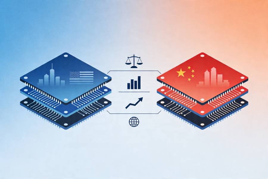
How to Decide: Local U.S. Manufacturer vs China Alternative
At this point, it should be clear that both U.S.-based multilayer PCB manufacturers and cost‑effective China alternatives have real strengths. The key question is not “which country is better,” but rather “which option matches my current project’s priorities?”
A simple way to approach this decision is to look at three dimensions:
- Risk and regulatory constraints
- Time and collaboration needs
- Budget and cost sensitivity
The comparison table below summarizes how U.S. manufacturers and China‑based partners like JHYPCB typically stack up for multilayer PCB projects.
| Factor / Priority | U.S.-Based Multilayer PCB Manufacturer | China Alternative (e.g., JHYPCB) |
|---|---|---|
| Regulatory constraints (ITAR, on‑shore) | Strong fit when U.S. production is mandatory or heavily preferred. | Generally not suitable for ITAR‑restricted work; better for commercial and industrial products. |
| Collaboration & time zone | Easier same‑day communication, on‑site visits, and audits in the U.S. | Remote collaboration with time zone differences; suitable when processes and communication are well established. |
| Logistics & shipping | Shorter domestic transit, no customs paperwork. | Slightly longer transit due to international shipping, but manageable with planning. |
| Cost for multilayer prototypes | Higher per‑unit cost and NRE, especially for complex stackups and small batches. | Significantly lower cost per build, allowing more prototype iterations within the same budget. |
| Cost for small & medium volumes | Often higher, reflecting domestic labor and overhead. | Typically more competitive pricing for multilayer PCBs at these volumes. |
| High layer count & HDI | Strong capabilities at many U.S. fabs, but cost may rise quickly with complexity. | Many Chinese fabs are highly optimized for complex multilayer and HDI at scale. |
| IP and legal jurisdiction | U.S. law and enforcement; easier to manage for some companies. | Requires clear NDAs and trust in the supplier’s track record and reputation. |
A Simple Decision Checklist
To make the choice more concrete, you can walk through a short checklist for your current project:
- Does your design fall under ITAR, defense, or strict local‑manufacturing rules?
- Yes: A U.S.-based multilayer PCB manufacturer is usually the only viable option.
- No: You can safely evaluate both domestic and China‑based suppliers.
- How sensitive is your schedule to shipping time?
- If you need ultra‑fast, last‑minute turns with minimal transit delay, a domestic manufacturer may be more convenient.
- If you can plan for a few extra days of transit, the cost savings from a capable China alternative can more than compensate.
- What is your prototype and NPI budget?
- Limited budgets and multiple expected respins strongly favor working with a cost‑effective partner like JHYPCB for multilayer prototypes.
- Larger budgets and high regulatory overhead may favor U.S. production for certain programs.
- How complex is your multilayer design?
- Very high layer counts, HDI, or exotic materials can be handled on both sides, but cost differences can be substantial; it is often worth getting quotes from both a U.S. supplier and a China‑based specialist.
- Do you foresee scaling from prototype to volume with the same supplier?
- If you want a single partner from first prototype through volume build for commercial products, a specialized multilayer manufacturer like JHYPCB can be very attractive.
- If you plan to eventually move high volumes into a separate contract manufacturing ecosystem, you may choose different suppliers for different phases.
A Hybrid Strategy for Many Teams
For many hardware companies, the most practical answer is not “U.S. or China,” but “U.S. and China.” A common hybrid approach looks like this:
- Use one or more U.S.-based multilayer PCB manufacturers for sensitive, regulated, or strategically important projects that demand on‑shore production and tight local collaboration.
- Partner with a cost‑effective multilayer PCB supplier like JHYPCB for commercial and industrial products, high‑layer‑count prototypes, and cost‑sensitive NPI where price and iteration speed are crucial.
By splitting work this way, you get the best attributes of each region: regulatory and logistical comfort from domestic suppliers, and high‑value multilayer capability with aggressive pricing from a specialized China alternative.
Conclusion: Shortlist the Best Options, Then Ask the Right Questions
Finding the “best” multilayer PCB manufacturer in the United States is ultimately less about rankings and more about fit. Large U.S. suppliers excel when you need on‑shore production, tight regulatory alignment, and real‑time collaboration for mission‑critical projects. Cost‑effective China alternatives, on the other hand, shine when you need to keep multilayer PCB costs under control, iterate quickly on prototypes, and still meet demanding technical requirements.
A practical way forward is to build a shortlist that includes both types of partners: one or two U.S.-based multilayer PCB manufacturers for programs that truly demand domestic production, and a specialized China‑based supplier like JHYPCB for commercial and industrial work where value, flexibility, and iteration speed matter most. Then, instead of relying on marketing promises alone, you can compare actual quotes, stackup proposals, DFM feedback, and sample builds for your own designs.
If you are currently evaluating options for your next multilayer PCB prototype or production run, JHYPCB would be happy to be part of that conversation. You can send your Gerber or ODB++ files for a no‑obligation multilayer PCB quote, ask our engineers to review your stackup, or simply discuss whether your project is a better fit for U.S. or China‑based manufacturing. This way, you are not just picking a name from a list—you are choosing a partner that understands your technical goals, your budget, and your long‑term roadmap.