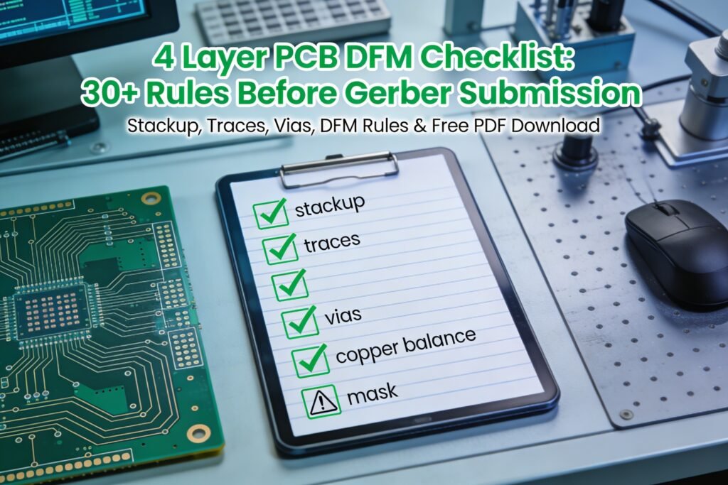
4 Layer PCB

4 Layer PCB Manufacturing Process: Step‑by‑Step Guide from Inner Layers to Final Testing

4 Layer PCB Manufacturing Process: Step‑by‑Step Guide from Inner Layers to Final Testing

This guide walks you through the full 4 layer PCB manufacturing process step by step—from FR4 material preparation and inner layer etching to lamination, drilling, plating, solder mask, and final electrical testing—so you can understand how design decisions and DFM rules affect cost, lead time, and reliability.

4 Layer PCB Manufacturing Process: Step‑by‑Step Guide from Inner Layers to Final Testing Read More »

4 layer vs 6 layer pcb

4 Layer vs 6 Layer PCB: How to Choose the Right Stackup for Your Design

Choosing between a 4 layer and 6 layer PCB is often a trade‑off between performance, EMI risk, routing freedom, and budget. This guide walks you through real‑world use cases, key comparison points, and a simple checklist you can use to decide whether 4 layers are enough or it is time to step up to a 6 layer stackup.

4 Layer vs 6 Layer PCB: How to Choose the Right Stackup for Your Design Read More »

Scroll to Top