Table of Contents
Quick Answer: Which 4 Layer PCB Thickness Do You Need?
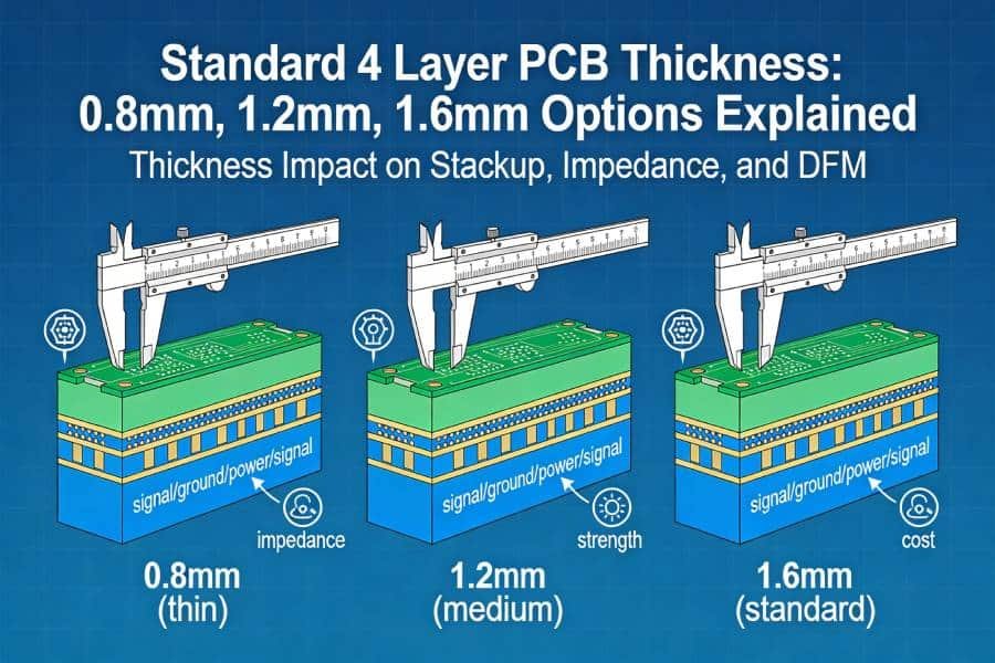
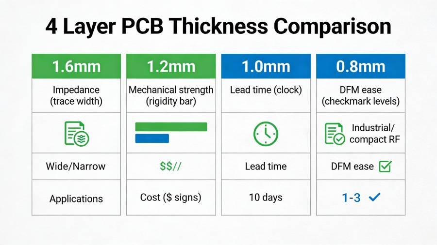
Standard Thicknesses at a Glance
If you are designing a 4 layer PCB and wondering about the right board thickness, here is the short version before we dive into details. Standard 4 layer PCB thickness options are driven by mechanical fit, impedance control, manufacturing cost, and application needs—1.6mm is the default for most projects, but thinner or thicker choices make sense in specific cases.
Quick selection guide:
| Thickness | Best For | Trade‑offs |
|---|---|---|
| 1.6mm (0.063″) | General industrial, embedded, IoT | Industry standard, lowest cost |
| 1.2mm (0.047″) | Compact devices, enclosures | Good impedance, slightly higher cost |
| 0.8–1.0mm | Ultra‑thin, high‑density | Best high‑freq, warpage risk |
| 2.0mm+ | Heavy mechanical loads | Highest strength, poor impedance |
Most engineers default to 1.6mm because it matches standard components, enclosures, and factory processes, offering the best balance of 4 layer PCB thickness for signal integrity, strength, and price. Use thinner boards when space is tight or frequencies demand tighter layer spacing, and thicker for vibration‑heavy environments.
Why Thickness Matters More Than You Think
4 layer PCB thickness is not just a mechanical spec—it directly affects dielectric spacing (impedance), mechanical rigidity (warpage/handling), thermal performance, and even assembly fit with connectors or standoffs. Choosing a non‑standard thickness can add 20–50% to cost and 5–10 days to lead time, so align with your stackup needs and manufacturer capabilities early.
This guide breaks down options, stackup implications, DFM rules, and real applications so you can select the optimal 4 layer PCB thickness options without guesswork. Curious about cost impact? See What Drives 4 Layer PCB Cost for pricing details.
Standard 4 Layer PCB Thickness Options Explained
1.6mm (0.063") – The Industry Default
1.6mm is the standard 4 layer PCB thickness for 90% of designs because it matches legacy components, enclosures, DIN rails, and global fabrication standards. This thickness provides excellent mechanical rigidity for handling, vibration resistance in industrial environments, and balanced dielectric spacing for impedance control (typically 50Ω microstrip with 5–6 mil traces).
Typical applications: Industrial controllers, embedded systems, IoT gateways, power supplies—anywhere reliability trumps thinness.
Pros: Lowest cost, shortest lead time, highest yield, standard stackups available.
Cons: Larger footprint, slightly wider traces for impedance (affects density).
Most factories offer 4 layer PCB 1.6mm stackup with 2116 prepreg (0.11–0.12mm dielectric) between layers, achieving total 1.57–1.60mm finished thickness.
1.2mm (0.047") – Compact and High‑Density
At 1.2mm, you get a thinner profile for space‑constrained designs while retaining good strength and standard processes. Tighter dielectric spacing (0.08–0.10mm prepreg) enables narrower traces for the same impedance, ideal for high‑density BGAs or compact enclosures.
Applications: Consumer electronics, medical wearables, automotive modules, drones.
Pros: 25% smaller than 1.6mm, better high‑freq performance, still volume‑friendly.
Cons: 10–20% higher cost than 1.6mm, slight warpage risk if asymmetric.
1.0mm (0.039") and Below – Ultra‑Thin Applications
0.8–1.0mm 4 layer PCBs push density and high‑frequency limits with very thin dielectrics (0.05–0.08mm), enabling 4–5 mil traces at 50Ω. Perfect for ultra‑compact or high‑speed designs, but requires precision fabrication.
Applications: Handheld devices, RF modules, aerospace, thin servers.
Pros: Maximal density, best impedance control.
Cons: Highest cost (+30–50%), warpage/handling risks, limited mechanical strength.
2.0mm+ – Heavy‑Duty and Mechanical Strength
Thicker boards (2.0–3.2mm) use heavier cores for extreme rigidity or high‑current power planes. Rare for signals but common in power electronics or harsh environments.
Applications: High‑power inverters, military, heavy machinery.
Pros: Superior strength, thermal capacity.
Cons: Poor high‑freq, custom process (+50% cost).
How PCB Thickness Affects Your 4 Layer Design
Impact on Impedance and Signal Integrity
4 layer PCB thickness has a direct, inverse relationship with trace impedance: thicker boards = larger dielectric spacing = higher impedance (for fixed trace width). This affects signal integrity because mismatches cause reflections, ringing, and data errors in high‑speed designs.
Example: To hit 50Ω microstrip impedance (Er=4.3, 1oz copper):
- 1.6mm thick: ~7 mil trace width (wider, lower density)
- 1.2mm thick: ~6 mil trace
- 0.8mm thick: ~4.5 mil trace (higher density)
Thinner 4 layer PCB thickness options enable tighter spacing for high‑frequency signals (>500 MHz) but demand finer features (increasing cost). For 100 Mbps Ethernet or USB 2.0, 1.6mm works fine; for Gigabit or RF, prefer 1.0–1.2mm.
Impedance vs Thickness Table (50Ω microstrip, Er=4.3):
| Total Thickness | Dielectric H (outer) | Trace Width (approx) | Signal Integrity Fit |
|---|---|---|---|
| 1.6mm | 0.12mm | 7.0 mil | Low/mid‑speed (<500 MHz) |
| 1.2mm | 0.10mm | 6.0 mil | Mid/high‑speed (<1 GHz) |
| 0.8mm | 0.06mm | 4.5 mil | High‑speed/RF (>1 GHz) |
Verify with your stackup calculator; always confirm with manufacturer for actual Er and H tolerances.
Mechanical Strength, Warpage, and Assembly
Thicker PCBs provide better rigidity for handling, vibration, and wave soldering, while thin boards risk flexing or warpage during reflow (especially asymmetric stackups).
- 1.6mm: Gold standard for industrial/automotive; fits standard DIN rails, standoffs.
- 1.2mm: Good balance for consumer; slight warpage risk if copper unbalanced.
- 0.8mm: Flexible for wearables; needs rigid fixtures in assembly.
- 2.0mm+: Heavy‑duty for power; poor for high‑density SMT.
Warpage rule: Keep outer layer copper density within ±10% of each other; use symmetric dielectrics. Thinner boards need high‑Tg FR4 to resist thermal stress.
Thermal Performance and Heat Dissipation
Thicker boards dissipate heat better through larger copper planes and mass, but thinner ones excel in compact cooling (convection/heatsinks). Via thermal relief and plane pours are key regardless.
- High power: 1.6–2.0mm + 2oz copper.
- Compact/high‑freq: 0.8–1.2mm + thermal vias arrays.
4 Layer PCB Stackup Thickness Breakdown
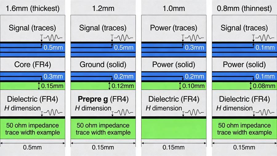
Core + Prepreg Combinations for Each Total Thickness
Once you choose a 4 layer PCB thickness, the real work is building a stackup with matching core and prepreg thicknesses that delivers your target impedance, plane spacing, and DFM compliance. Factories standardize these combinations for reliability and cost—custom mixes add expense and risk.
Standard 4 layer PCB stackup thickness combinations (1oz copper, FR4):
| Total Thickness | Typical Stackup | Core Thicknesses | Prepreg (x3) | Dielectric H (outer) | Notes |
|---|---|---|---|---|---|
| 1.6mm | S/G/P/S | 0.8mm core | 0.11mm 2116 x3 | 0.12mm | Default, ±0.10mm tolerance |
| 1.2mm | S/G/P/S | 0.6mm core | 0.08mm 1080 x3 | 0.09mm | Compact, good impedance |
| 1.0mm | S/G/P/S | 0.4–0.5mm core | 0.06mm 106 x3 | 0.07mm | High‑density, tight tolerance |
| 0.8mm | S/G/G/S | 0.3mm core | 0.05mm thin x3 | 0.06mm | RF/flex, warpage risk |
These use standard materials like 2116/1080 prepreg for 1.6/1.2mm—your 4 layer pcb 1.6mm stackup typically finishes 1.57–1.60mm after lamination/plating. Thinner boards (<1.0mm) may require high‑Tg or low‑CTE cores to prevent delamination.
Standard Factory Stackups (with Examples)
Most manufacturers publish standard 4 layer stackup tables matching common thicknesses—use these to avoid custom tooling. For standard 4 layer PCB thickness like 1.6mm:
Example 1.6mm Stackup (S/G/P/S):
- Layer 1 (top signal): 1.4oz finished
- Prepreg 2116: 0.11mm (H=0.12mm)
- Layer 2 (GND): 1oz
- Core 0.8mm
- Layer 3 (PWR): 1oz
- Prepreg 2116 x2: 0.22mm
- Layer 4 (bottom signal): 1.4oz
Impedance: 50Ω microstrip top/bottom (~7 mil trace); 100Ω diff pair (~10 mil spacing).
For 1.2mm, scale down to 1080 prepreg (0.08mm) and 0.6mm core. See our full 4 Layer PCB Stackup Guide for diagrams and impedance calcs.
Request your factory’s table early—standard combinations cut cost 15–25% vs custom.
Cost, Lead Time, and DFM Considerations
Standard vs Custom Thickness Pricing
Standard 4 layer PCB thickness like 1.6mm and 1.2mm use factory‑optimized core/prepreg combos, keeping costs low and yields high. Custom thicknesses (e.g., 1.35mm) require special laminations, adding 20–50% to price and 3–7 days to lead time.
Typical pricing trends (100x100mm, 4 layer, standard features, prototype qty):
| Thickness | Relative Cost (vs 1.6mm) | Lead Time | Why the Difference |
|---|---|---|---|
| 1.6mm | 100% (baseline) | 3–5 days | Standard cores/prepregs, high volume |
| 1.2mm | 110–120% | 4–6 days | Thinner materials, tighter tolerance |
| 1.0mm | 130–150% | 5–7 days | Precision lamination, warpage control |
| 0.8mm | 150–200% | 7–10 days | Custom thin cores, handling challenges |
| Custom | +20–50% | +3–7 days | Non‑standard tooling |
What Drives 4 Layer PCB Cost? covers full pricing, but thickness alone can swing quotes 30%—always request 4 layer pcb thickness cost breakdown.
DFM Rules for 4 Layer PCB Thickness
4 layer pcb thickness dfm ensures fabricability:
- Aspect ratio: Drill depth/diameter ≤10:1 (1.6mm board → ≥0.16mm drill).
- Copper balance: ±10% between symmetric layers to prevent warpage.
- Tolerance: ±10% standard (±0.16mm for 1.6mm); tighter adds cost.
- Symmetry: Equal prepregs top/bottom for flatness.
Thin boards (<1.0mm) need high‑Tg FR4 and handling precautions; thick (>2.0mm) limit via plating reliability.
Checklist: Selecting the Right Thickness
4 layer pcb thickness selection checklist:
- Matches enclosure/mechanical specs?
- Impedance achievable with standard traces (calc H)?
- Aspect ratio ≤10:1 for vias?
- Standard factory combo available (no custom lamination)?
- Copper symmetric (±10%)?
- Cost/lead time fits project timeline?
Run this with your stackup sim. Upload for free thickness + DFM review—we confirm optimal combo before production.
Real‑World Applications and Examples
Thickness Choices in Action
Standard 4 layer PCB thickness shines in specific scenarios—here are common applications with optimal choices and why they work:
Industrial Control (1.6mm): PLCs, motor drivers, HMIs use 1.6mm for DIN rail fit, vibration resistance, and wave soldering compatibility. Thick core handles thermal cycling; standard stackup ensures low cost.
IoT/Embedded (1.2–1.6mm): Gateways, sensors favor 1.2–1.6mm for enclosure fit and balanced impedance. 1.2mm suits compact battery‑powered nodes; 1.6mm for mains‑powered reliability.
Communication Modules (1.0–1.2mm): Ethernet/WiFi modules need thin 4 layer pcb thickness for high speed (tighter dielectric for 50Ω at narrow traces). 1.0mm excels for RF; 1.2mm balances density/cost.
Power Electronics (2.0mm+): Inverters, converters use thick boards for current capacity and heatsink mounting.
Application Matrix:
| Application | Recommended Thickness | Key Reason | Related Guide |
|---|---|---|---|
| Industrial Control | 1.6mm | Mechanical strength, standard fit | Design Guidelines |
| IoT Devices | 1.2–1.6mm | Enclosure + impedance | Stackup Guide |
| Networking | 1.0–1.2mm | High‑speed density | 4 vs 6 Layer |
| Power Supplies | 1.6–2.0mm | Thermal/strength | Cost Factors |
These examples show 4 layer pcb thickness selection aligns with project constraints. Upload specs for thickness recommendation.
FAQ: Common Questions About 4 Layer PCB Thickness
1.6mm (0.063") is the global industry default for its balance of strength, cost, and compatibility with standard components/enclosures. Most factories optimize stackups around this thickness.
Yes, for ultra‑compact or high‑frequency designs, but expect 30–50% higher cost, warpage risks, and tighter DFM rules. Ideal for RF modules or wearables.
Thicker boards (1.6mm) require wider traces for 50Ω (~7 mil); thinner (0.8mm) allow narrower (~4.5 mil) for higher density but demand precision fab. See our 4 Layer PCB Stackup Guide for calcs.
1.6mm for DIN rail fit, vibration resistance, and thermal reliability in PLCs/motor drivers.
Yes, thinner (<1.0mm) risks more warpage; ensure symmetric copper (±10%) and high‑Tg FR4. Standard 1.6mm has minimal issues.
Need Help Choosing Your 4 Layer PCB Thickness?
Standard 4 layer PCB thickness decisions impact impedance, strength, cost, and manufacturability—get it right from the start with our guides:
- 4 Layer PCB Stackup Guide – Stackup + thickness details
- 4 Layer PCB Design Guidelines – Layout rules
- What Drives 4 Layer PCB Cost? – Pricing factors
- 2 vs 4 Layer & 4 vs 6 Layer – Layer decisions
Unsure about 0.8mm vs 1.6mm for your project? Upload Gerbers/specs for free thickness analysis + DFM review + quote. We confirm optimal 4 layer pcb thickness options, stackup, and cost before production. Start your review.