Table of Contents
Quick Answer: When to Choose 4 vs 6 Layers
Who This Guide Is For
If you are hesitating between a 4 layer vs 6 layer PCB for your next project, you are exactly who this guide is written for. It is aimed at hardware engineers who own the schematic and layout, as well as project managers and purchasing teams who must balance performance, risk, and budget. Whether you are designing an industrial control board, a compact IoT device, or a high‑speed communication product, choosing the right PCB layer count early can save you multiple spins, weeks of delay, and a lot of debugging time. Instead of only comparing theoretical stackups, we will focus on how 4 layer and 6 layer PCBs behave in real‑world designs and what that means for your schedule and total cost.
TL;DR: 4 Layer vs 6 Layer PCB in One Look
If you need a quick answer before diving into the details, here is the short version of 4 layer vs 6 layer PCB and when to use each option. Use it as a first filter, then read the rest of the article to validate your decision with a more detailed checklist.
- Stay with a 4 layer PCB if your design runs mostly at low to mid‑speed digital interfaces (for example standard UART, SPI, I²C, low‑speed USB, 10/100 Mbps Ethernet), your component density is moderate, and your board size is not extremely constrained. A standard 4 layer PCB stackup with two signal layers and solid power/ground planes will usually give you a good balance between routing space, basic signal integrity, and cost. For many industrial control, general consumer, and IoT products, 4 layers are more than enough when the layout is done carefully. Learn more in our full 4 Layer PCB Stackup Guide.
- Consider moving to a 6 layer PCB if you have multiple high‑speed differential pairs, dense BGAs or fine‑pitch packages, strict EMI/EMC requirements, or several power rails that must remain very stable. In these cases, a 6 layer PCB stackup with additional signal and reference planes gives you more routing freedom, better controlled impedance, and stronger EMI performance, especially in compact boards where you cannot increase the PCB size. For applications such as communication and networking devices, high‑speed embedded systems, or FPGA‑based designs, a 6 layer PCB often pays off in fewer layout compromises and faster compliance testing.
- From a cost perspective, a 6 layer PCB will normally be more expensive than a 4 layer PCB because of the extra materials, lamination cycles, and increased process complexity. However, when you factor in the risk of failed EMC tests, extra PCB spins, or hours spent fighting routing congestion on a 4 layer board, the total project cost of “staying cheap” can easily exceed the price difference between 4 and 6 layers. In other words, the right question is not only “how much more does a 6 layer PCB cost?” but “how much engineering and schedule risk does it remove for this particular design?”
- If you are still not sure after reading this section, a practical approach is to treat 4 layers as the default starting point, then check your interfaces, density, EMI requirements, and budget against the decision checklist later in this article. If more than one of those dimensions looks “high‑risk” for a 4 layer board, it is usually safer to plan for a 6 layer PCB from the beginning rather than upgrading after your first prototype fails.
Basics: What’s the Difference Between 4 and 6 Layer PCBs?
Typical 4 Layer PCB Stackup and Where It Fits
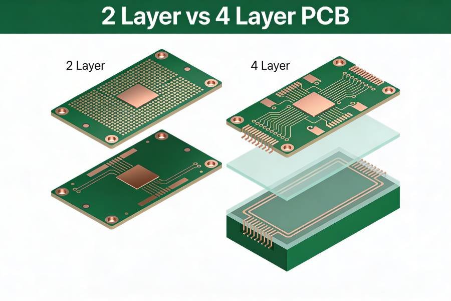
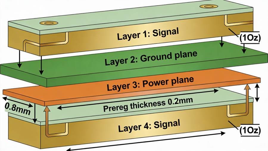
A typical 4 layer PCB has two outer signal layers and two inner planes that are usually used for power and ground, for example a stackup like Signal / Ground / Power / Signal. This standard 4 layer PCB stackup gives you solid reference planes for most digital designs while keeping the total thickness, cost, and manufacturing process within a very familiar window for PCB factories.
In practice, 4 layer PCBs are a good fit for medium‑complexity designs where signal speeds are low to moderate and the board size is not extremely constrained. Industrial control boards, many IoT devices, home appliances, and general embedded systems often stay at four layers because you can still route all nets cleanly while maintaining acceptable signal integrity and EMI performance. When a 2 layer board becomes too noisy or too crowded, moving up to a 4 layer PCB is usually the first and most cost‑effective step.
If your current project falls into this category, a well‑planned 4 layer stackup can give you surprisingly good results. By keeping one solid ground plane and one solid power or mixed plane inside, you support controlled impedance traces on the outer layers and provide short, predictable return paths for digital signals. When you combine this with clean layout practices, you often do not need to jump to a 6 layer PCB just to “play it safe”.
Below is a common example of a 4 layer PCB stackup:
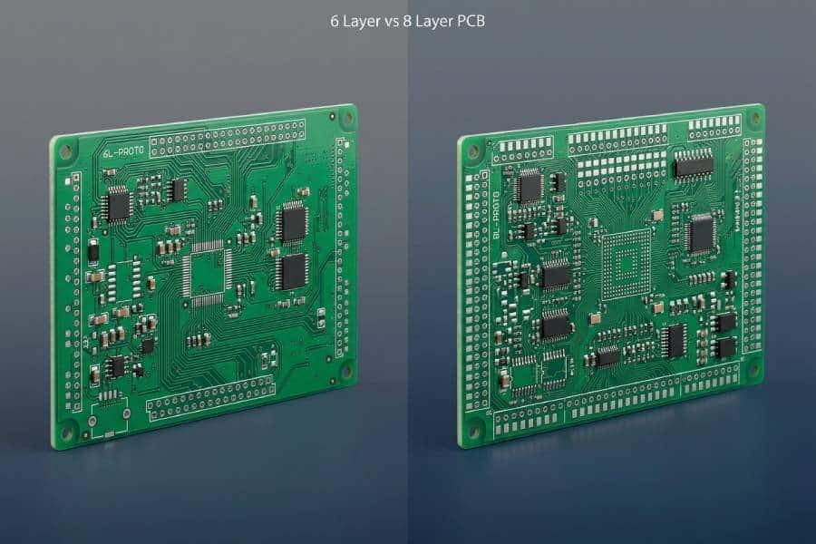
Typical 6 Layer PCB Stackup and Where It Shines
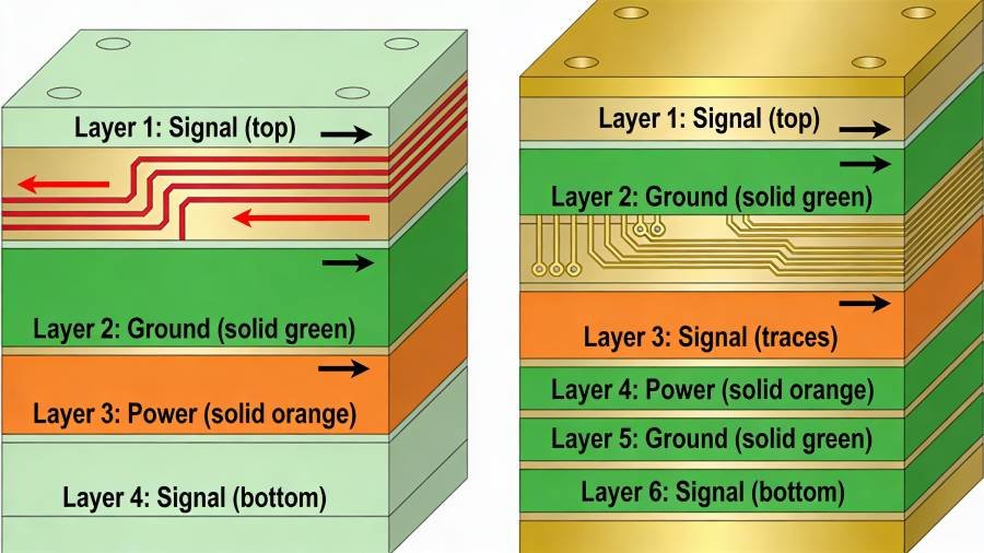
A standard 6 layer PCB adds two more copper layers compared to four layers, and a common stackup might look like Signal / Ground / Signal / Power / Ground / Signal. In this kind of 6 layer PCB stackup, every high‑speed signal layer sits close to a solid reference plane, and the power and ground planes can be placed next to each other to improve decoupling and reduce noise. These extra layers give you more routing channels and much more freedom to separate noisy and sensitive circuits.
Because of this structure, 6 layer PCBs are widely used in designs that carry high‑speed differential pairs, dense BGAs, or multiple interfaces that must pass strict EMI/EMC tests. Typical examples include communication and networking devices, high‑speed computing boards, complex embedded systems, and many FPGA or high‑end MCU designs. In these products, the additional cost of moving from 4 to 6 layers is often justified by better signal integrity, easier routing, and fewer surprises during compliance testing.
For procurement and project managers, the key takeaway is that a 6 layer PCB is not just “two more copper layers”. It is a different level of design flexibility: more room to route critical nets, more options to shield sensitive analog circuits, and a stronger power distribution network for high‑current or noise‑sensitive loads. When your engineering team says “this really should be a 6 layer design”, it usually means they want to reduce layout compromises that could otherwise turn into late‑stage issues.
How Extra Layers Change Performance, Cost, and Manufacturability
From a performance point of view, adding layers mainly improves three aspects: signal integrity, EMI/EMC behavior, and power distribution. With more signal layers and more planes, you can keep controlled impedance traces shorter and cleaner, provide continuous reference planes under high‑speed routes, and build a tighter, lower‑impedance power‑ground pair. All of this translates into cleaner waveforms, fewer crosstalk issues, and a better chance to meet high‑speed interface and EMC requirements on the first try.
The trade‑off is that a 6 layer PCB generally has higher material and process costs and slightly more complex manufacturability compared to a 4 layer PCB. Your fabricator must press more cores and prepregs, control layer registration more tightly, and maintain impedance across more interfaces. For established PCB manufacturers, both 4 layer and 6 layer boards are standard work, but the additional steps and yield considerations are the main reasons why a 6 layer PCB costs more than a 4 layer PCB of similar size and technology.
What matters for your project is how these differences interact with your constraints. If a 4 layer board forces the layout team into risky compromises—narrow return paths, long stubs on high‑speed nets, fragmented ground planes—saving on layers can actually increase your total cost through extra spins and debug time. On the other hand, if your interfaces are modest and the board has comfortable space, a well‑designed 4 layer PCB can deliver reliable performance without the added expense and complexity of six layers.
Here is how the stackups look side by side:
Key Comparison: 4 Layer vs 6 Layer PCB
Side‑by‑Side Overview
When you compare a 4 layer vs 6 layer PCB, the most important differences show up in routing space, signal integrity, EMI/EMC behavior, power distribution, and manufacturing cost. A 4 layer PCB gives you two signal layers and two planes, which is usually enough for moderate‑complexity designs where the board is not extremely compact. A 6 layer PCB adds more internal signal and plane layers, so you gain routing channels and better isolation between noisy and sensitive circuits, which becomes critical in high‑speed or very dense layouts.
For many products, a 4 layer PCB is the sweet spot between performance and budget, especially when the design does not push the limits of interface speed or EMI requirements. However, once you start working with multiple high‑speed buses, high‑pin‑count devices, or strict regulatory tests, a 6 layer PCB offers more options to control impedance, shorten return paths, and separate different functional blocks. Thinking in terms of “design headroom” rather than just layer count helps you choose the right option for your specific project.
Factor‑by‑Factor Comparison
| Factor | 4 Layer PCB | 6 Layer PCB |
|---|---|---|
| Stackup structure | 2 signal layers, 1 power plane, 1 ground plane; typical stackup like Signal / GND / PWR / Signal. | 3–4 signal layers plus 2–3 power/ground planes; common stackup like Signal / GND / Signal / PWR / GND / Signal. |
| Routing space | Enough for moderate complexity, may be tight for dense BGAs or 4 layer pcb routing limitations | More routing channels on internal layers, easier to handle dense BGAs, mixed‑speed buses, and tight enclosures. |
| Signal integrity | Good for low‑ to mid‑speed interfaces with careful layout and solid reference planes. | Better for high‑speed and high‑frequency signals thanks to more controlled impedance routes and continuous reference planes. |
| EMI/EMC behavior | Clearly better than 2‑layer boards, but limited shielding options and fewer planes for isolation. | Stronger EMI control with extra planes used as shields and better separation of noisy and sensitive areas. |
| Power distribution | Single power plane can support a few rails with moderate current; PDN performance depends heavily on layout. | Multiple planes and closer power‑ground pairing provide lower‑impedance PDN, ideal for high current and many rails. |
| Board size & density | Works well when the PCB area is not extremely constrained and component density is moderate. | Better suited for compact, high‑density designs where increasing board size is not an option. |
| Typical applications | Industrial control, general consumer products, many IoT devices, mid‑range embedded systems. | Communication and networking equipment, high‑speed computing boards, complex embedded and FPGA‑based systems. |
| Cost & manufacturability | Lower material and process cost, simpler to fabricate, typically shorter lead time. | Higher cost due to extra layers and lamination cycles, more complex but still standard for professional fabricators. |
For hardware engineers, this table highlights where a 4 layer PCB starts to feel “tight”: when routing congestion appears, when you struggle to maintain solid reference planes, or when high‑speed signals are forced into awkward detours. For purchasing and project managers, the key message is that the extra cost of a 6 layer PCB buys you routing margin, better EMI behavior, and a stronger power network, which can reduce the risk of failed prototypes and schedule slips.
Real‑World Design Examples
Imagine you are designing an industrial control board with a mid‑range MCU, a few communication interfaces such as RS‑485 and 10/100 Ethernet, and moderate component density. In this scenario, a well‑planned 4 layer PCB with a standard stackup and clean layout practices is usually sufficient. You benefit from lower cost and simpler manufacturing while still getting stable signal integrity and EMI performance that meets most industrial requirements.
Now consider a compact communication and networking device with multiple high‑speed Ethernet ports, a high‑pin‑count processor or FPGA, and strict EMC certification targets. In that case, a 6 layer PCB gives you the extra routing space and dedicated planes needed to keep differential pairs short, maintain controlled impedance, and separate noisy switch‑mode power stages from sensitive receivers. Trying to squeeze such a design onto a 4 layer PCB often leads to fragmented ground planes, long return paths, and unpredictable EMI issues that are expensive to fix late in the project.
There are also hybrid situations where the choice is not obvious from the beginning. For example, a design might start as a 4 layer PCB during early prototyping, but once the feature set and performance targets are fully defined, the team realizes that moving to six layers will reduce risk and simplify layout. In these cases, involving your PCB manufacturer early and sharing your planned stackup, interfaces, and size constraints can help decide whether a 4 layer or 6 layer PCB is the better long‑term choice for both performance and cost.
How to Decide: A Practical Checklist
Check 1 – Signal Speeds and Interfaces
Start by listing all the key interfaces on your board and their approximate data rates. If your design mainly uses low‑ to mid‑speed signals—such as UART, SPI, I²C, CAN, low‑speed USB, or 10/100 Mbps Ethernet—a well‑designed 4 layer PCB is usually sufficient, especially when the board size is reasonable and routing is not extremely dense. Explore our 4 Layer PCB service page for standard capabilities and pricing.
However, once you introduce multiple high‑speed differential pairs, high‑frequency clocks, or links like USB 3.x, Gigabit Ethernet, high‑speed SerDes, or fast memory buses, the advantages of a 6 layer PCB become more obvious. Extra internal signal layers, combined with solid reference planes, make it much easier to maintain controlled impedance and short, clean return paths, which directly affects signal integrity and your chances of passing high‑speed compliance tests on the first try.
Check 2 – Component Density and Board Size
Next, look at how much “room” you have: overall PCB dimensions, number of components, and especially pin‑dense devices such as BGAs, fine‑pitch connectors, and large FPGAs or SoCs. If your layout can be completed on two outer signal layers with only moderate use of vias and without breaking up your reference planes, a 4 layer PCB often remains the most cost‑effective option.
By contrast, if the combination of a small board outline and high component density forces you into heavy via usage, long detours, and narrow routing channels, that is a strong sign that you may need six layers. A 6 layer PCB gives you additional internal routing layers that relieve congestion around dense BGAs and allow you to keep planes more continuous, which improves both signal integrity and manufacturability.
Check 3 – EMI/EMC Requirements and Operating Environment
EMI/EMC is often where the real difference between a 4 layer vs 6 layer PCB shows up. If your product will operate in relatively benign environments and is not subject to very strict EMC standards, a 4 layer board with a solid ground plane, good return paths, and proper filtering can perform very well. Many industrial control and general embedded systems successfully pass EMC tests on four layers when the layout is disciplined.
On the other hand, products that must pass demanding EMC standards or operate in noisy environments—communication equipment, high‑speed networking devices, automotive or medical electronics—benefit a lot from the extra planes and routing options of a 6 layer PCB. Additional ground and power planes can be used as shields and allow you to partition noisy and sensitive circuits more cleanly, which reduces both radiated emissions and susceptibility to external noise.
Check 4 – Power Rails and Current Levels
Consider how many different power rails you have, their voltage levels, and the maximum currents they need to carry. A simple design with one or two moderate‑current rails is usually fine on a 4 layer PCB, as long as you allocate enough plane area and place decoupling capacitors correctly. In these cases, the inner power‑ground pair on a standard 4 layer stackup can provide a solid foundation for power distribution.
When your design includes multiple rails, high‑current loads, or very noise‑sensitive analog sections, a 6 layer PCB offers more freedom to build a robust power distribution network. You can dedicate more area to power and ground, place power‑ground pairs closer together for lower impedance, and separate noisy switching regulators from quiet analog or RF sections more effectively. This is especially important in high‑density boards where you cannot simply “make the board bigger” to gain extra copper area.
Check 5 – Budget, Volume, and Risk Tolerance
Layer count always has to be balanced against budget and volume. A 4 layer PCB will almost always be cheaper than a 6 layer PCB of similar size and technology, and for high‑volume, cost‑sensitive products this difference can matter a lot. If your design is technically comfortable on four layers, there is no reason to pay for extra copper just because higher layer counts “feel more professional”.
At the same time, it is important to look at total project cost, not only the price per panel. If pushing the design onto four layers forces your engineers into aggressive routing compromises, that can lead to extra debug time, failed EMC tests, or even additional PCB spins, all of which are more expensive than the incremental price of a 6 layer PCB. For low‑volume or high‑value products, paying a bit more per board to reduce technical risk is often the smarter financial decision.
A Simple Decision Matrix
You can summarize the previous checks using a simple matrix. The more items fall on the “high” side, the more likely you should choose a 6 layer PCB from the start rather than trying to “upgrade later”.
- If your signals are low‑ to mid‑speed, component density is moderate, EMI requirements are standard, and you have only a few power rails, a 4 layer PCB is usually the right default.
- If you have one or two “borderline” factors—such as slightly higher speeds or a somewhat compact board—you may still stay with four layers, but it is wise to discuss stackup options and constraints with your PCB manufacturer early.
- If several factors are clearly high‑risk (multiple high‑speed interfaces, dense BGAs, strict EMC targets, many rails, and tight space), planning for a 6 layer PCB will give your design team more margin and usually reduce the overall risk and time‑to‑market.
If, after walking through this checklist, you are still not confident about staying with four layers, a practical next step is to share your schematic, preliminary stackup idea, or existing Gerber files with your PCB manufacturer. An experienced engineering team can review your requirements and tell you honestly whether a 4 layer or 6 layer PCB is the safer choice for your specific project and industry.
Cost Considerations: How Much More Does 6 Layers Really Cost?
What Actually Drives Multilayer PCB Cost
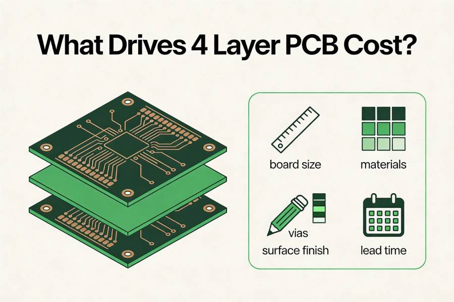
When you compare the cost of a 4 layer vs 6 layer PCB, the layer count is only one of several important cost drivers. Board size, material type, copper thickness, minimum trace/space, via technology, surface finish, and lead time all have a significant impact on the final price.
From a manufacturing point of view, each additional layer adds more core and prepreg material, extra lamination cycles, longer drilling and imaging steps, and tighter registration requirements. That is why PCB price does not scale linearly with the number of layers; a 6 layer PCB is not just “50% more expensive” than a 4 layer PCB, it can be 30–40% higher or more depending on stackup, tolerances, and technology choices.
Typical Cost Difference Between 4 Layer and 6 Layer PCBs
Industry data and manufacturer price guides show that moving from a 4 layer PCB to a 6 layer PCB often increases bare board cost on the order of 30–40% for the same size and similar technical requirements. For example, some public price references indicate that a 4 layer board may fall into a certain cost range per square centimeter, while a 6 layer board of similar specification sits in a higher band because of the extra copper layers and process complexity.
It is also common to see that 4–6 layer PCBs remain in the “economical and standard” category, while 8+ layer PCBs jump into a noticeably more expensive and process‑sensitive range. In other words, six layers are often viewed as a practical sweet spot: more expensive than four layers, but still far more cost‑effective than very high layer counts that are typically reserved for cutting‑edge computing, telecom, or aerospace systems.
Because real prices depend heavily on exact stackup, quantity, and technical specs, it is not realistic—or good for SEO—to promise fixed numbers in a blog post. Instead, you can explain the relative trends and then invite readers to request a customized 4 vs 6 layer cost comparison based on their Gerber files or stackup proposal.
Why “Cheaper per Board” Is Not Always Cheaper Overall
When deciding between a 4 layer vs 6 layer PCB, it is easy to focus on the price per board and forget about engineering time, test cycles, and schedule risk. A 4 layer PCB is cheaper to fabricate, but if squeezing a complex design into four layers leads to routing compromises, fragmented planes, or marginal signal integrity, you may end up paying more in extra debug time and failed EMC tests than you saved on the bare board.
For prototypes and low‑volume, high‑value products, the extra cost of a 6 layer PCB is often justified by a smoother design process and a higher chance of first‑pass success. Even in mid‑volume production, reducing the number of redesigns and field issues can easily offset the incremental price of going from four layers to six. Thinking in terms of “total cost of ownership” rather than just “PCB price” helps both engineers and purchasing teams make more balanced decisions.
How Good Stackup and DFM Can Control 6 Layer PCB Cost
If your checklist clearly points toward using a 6 layer PCB, there are still many ways to keep the cost under control. Choosing a stackup that matches your manufacturer’s standard materials and thicknesses, avoiding unnecessarily tight line/space rules, minimizing the use of blind or buried vias, and selecting a suitable surface finish can all make a noticeable difference in price. Designs that stay within a fabricator’s preferred process window typically enjoy better yields, shorter lead times, and more stable pricing.
The most effective approach is to discuss your planned 4 or 6 layer stackup with your PCB partner early in the design phase. By sharing your target layer count, board thickness, impedance requirements, and any special reliability needs, you give the factory a chance to suggest cost‑optimized stackups and design‑for‑manufacturing (DFM) improvements before you lock the layout. If you are currently comparing a 4 layer vs 6 layer PCB for a new project, you can send your schematic or preliminary Gerber files to our engineering team and request a side‑by‑side cost and risk evaluation tailored to your specific design.
Design Tips: Making the Most of 4 and 6 Layers
If You Stay with 4 Layers: Best‑Practice Layout Tips
On a 4 layer PCB, the most important decision is to use a solid reference plane directly under your main signal layer, typically a stackup like Signal / Ground / Power / Signal. This structure lets you route critical nets on the outer layer with a continuous ground plane just beneath them, which keeps return paths short and helps with both signal integrity and EMI.
When routing, try to keep high‑speed or noisy signals on the layer adjacent to the ground plane and avoid cutting up that plane with unnecessary splits or large voids. Minimize via count on critical nets, keep differential pairs tightly coupled, and route orthogonally between layers to reduce crosstalk. For power distribution, reserve enough area on the inner power plane, place decoupling capacitors as close as possible to IC power pins, and provide short, low‑inductance connections back to the ground plane.
If you are pushing the limits of what a 4 layer board can handle—high‑density components, mixed‑signal sections, or borderline EMI margins—it becomes even more important to plan the stackup and routing strategy early. Sharing your intended 4 layer PCB stackup with your manufacturer before layout starts can help you avoid combinations of materials and thicknesses that make impedance control or manufacturing more difficult than necessary.
If You Move to 6 Layers: Common Stackups and Pitfalls
With a 6 layer PCB, you gain more routing options and extra planes, but you also have more ways to create unnecessary complexity if the stackup is not planned carefully. Common 6 layer stackups include structures such as Signal / Ground / Signal / Power / Ground / Signal or variants where power and ground planes are paired to improve decoupling and EMI performance. The key idea is to keep as many signal layers as possible directly adjacent to a solid reference plane so that critical traces always have a clean, predictable return path.
One frequent pitfall is placing two high‑speed signal layers directly adjacent to each other with no plane in between, which increases the risk of crosstalk and makes return currents less controlled. Another is over‑fragmenting power or ground planes with unnecessary splits, which can defeat the purpose of moving to six layers in the first place. A well‑designed 6 layer PCB stackup will typically dedicate at least one inner layer to power and two to ground, using the remaining layers for routing critical signals and less sensitive nets.
When you plan a 6 layer board, think in terms of zones: group noisy switching regulators together and keep them on layers with strong return paths, place sensitive analog or RF sections above continuous planes, and route fast digital buses on layers with clearly defined impedance. Before you start layout, it is worth sending your proposed 6 layer stackup to your PCB manufacturer and asking for feedback on material choices, layer order, and thicknesses; small changes at this stage can improve both performance and cost.
When to Involve Your PCB Manufacturer Early
Regardless of whether you choose a 4 layer or 6 layer PCB, early communication with your fabricator can remove a lot of uncertainty from the design process. Manufacturers know which 4 layer and 6 layer stackups are standard in their production lines, which material combinations give stable impedance and good yields, and where the real cost breakpoints are for different layer counts and design rules.
From a practical point of view, a simple way to reduce risk is to share three things before you finalize the layout: your target layer count (4 vs 6 layers), the intended board thickness, and any special requirements such as controlled impedance or tight EMI/EMC margins. With that information, your PCB partner can suggest stackup options, point out potential manufacturing issues, and even give you a comparative quote so you can see the real cost difference between a 4 layer PCB and a 6 layer PCB for your specific design. If you are currently evaluating both options, sending your preliminary schematic or Gerber files for a quick review can help you decide with confidence before you commit to one direction.
FAQ: Common Questions About 4 Layer vs 6 Layer PCBs
Not necessarily. A 6 layer PCB offers more routing space, better signal integrity, and stronger EMI control, but it also costs more and is not required for every design. If your interfaces are low‑ to mid‑speed, your board is not extremely dense, and EMI requirements are moderate, a well‑designed 4 layer PCB is often the more efficient and economical choice.
For truly high‑speed interfaces such as USB 3.x, PCIe, SerDes, or Gigabit Ethernet, a 6 layer PCB usually makes it much easier to maintain controlled impedance, provide continuous reference planes, and manage EMI/EMC. In some borderline cases a very careful 4 layer design can work, but it tends to involve tighter layout constraints and higher risk, so many teams prefer six layers for these applications.
There is no single percentage that fits every case, but many manufacturing references show that 6 layer PCBs often cost roughly 30–40% more than comparable 4 layer PCBs of the same size and technology level. The exact difference depends on stackup, materials, design rules, and order volume, which is why it is best to request a 4 vs 6 layer cost comparison based on your actual files.
Yes, but changing the layer count after the first prototype can require significant layout rework and may affect mechanical constraints such as board thickness and connector positions. A better approach is to estimate your required PCB layers early using the kind of checklist in this article, then validate that choice with your PCB manufacturer before freezing the design.
When you are pushing a 4 layer PCB, a common recommendation is to use a stackup like Signal / Ground / Power / Signal and to keep the ground plane as continuous as possible. This structure allows you to route critical signals on the outer layer adjacent to the ground plane and use the inner power plane mainly for low‑impedance power distribution and local reference.
A widely used starting point for many 6 layer PCBs is a stackup such as Signal / Ground / Signal / Power / Ground / Signal, which keeps each signal layer next to a solid reference plane and pairs power with ground for better decoupling. Your final stackup should still be confirmed with your PCB manufacturer, who can align it with their standard materials, impedance models, and cost structure.
If even a 6 layer PCB cannot provide enough routing channels, clean reference planes, or isolation for very complex high‑speed or mixed‑signal designs, you may need to consider 8 or more layers. This is common in advanced computing, telecom backplanes, or very dense FPGA boards, but for most industrial, IoT, and general embedded products, four or six layers are usually sufficient when the stackup and layout are well planned.
At a minimum, you should share your target layer count (4 or 6), expected board size and thickness, key interfaces and their speeds, any controlled‑impedance requirements, and your estimated production volume. If you already have a draft stackup, schematic, or preliminary Gerber files, sending those as well allows the engineering team to suggest a specific 4 layer or 6 layer PCB stackup and provide a realistic cost and risk comparison for your project. Get started on our 4 Layer PCB service page.
Still Not Sure? Send Us Your Stackup or Gerbers
Choosing between a 4 layer and 6 layer PCB is rarely just a theoretical exercise; it depends on your actual interfaces, layout constraints, EMI targets, and budget. If you have walked through the checklist in this article and still feel that your design sits somewhere in the gray area, it is a good moment to involve your manufacturer instead of guessing alone.
You do not need a final layout to get useful feedback. Sharing your schematic, a block diagram, or a preliminary stackup proposal is often enough for an experienced engineering team to tell you whether a 4 layer PCB is safe or a 6 layer PCB will reduce risk and rework. Based on your files and requirements, we can also prepare a like‑for‑like 4 vs 6 layer PCB cost comparison so you see the real impact on price, not just general percentages.
If you are currently planning a new industrial control, IoT, communication, or embedded project and are unsure which direction to take, feel free to send us your stackup idea or Gerber files. We will review your design, suggest a practical 4 or 6 layer PCB stackup, and highlight any obvious layout or manufacturability risks before you commit to the next prototype. This way, your layer‑count decision is supported by both engineering insight and real manufacturing data, not just rules of thumb.