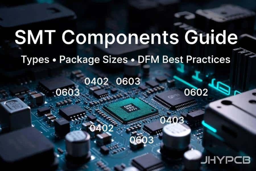
Table of Contents
Introduction: The Evolution of Soldering in PCBA
The Global Pivot: Navigating Lead-Free and Leaded Solder
In the realm of Surface Mount Technology (SMT) assembly, the choice between leaded and lead-free solder is no longer just a technical preference—it is a critical business decision influenced by international law, environmental ethics, and long-term hardware reliability.
For decades, the eutectic Sn63/Pb37 (63% tin, 37% lead) alloy was the “gold standard” of the electronics industry due to its low melting point and superior wetting properties. However, the landscape shifted dramatically in 2006 with the enforcement of the RoHS (Restriction of Hazardous Substances) directive. This sparked a global transition toward Lead-Free (Pb-Free) alternatives, such as the SAC305 (Tin-Silver-Copper) alloy, fundamentally changing how PCBs are designed, soldered, and inspected.
At a Glance: Key Differences
To understand the impact on your next PCBA project, we must look at the two primary dimensions where these materials diverge:
- Compliance: While Lead-Free is mandatory for most consumer electronics worldwide, Leaded solder remains a staple in specific “high-reliability” sectors, including aerospace and defense, under strict exemptions.
- Performance: Lead-Free alloys demand higher processing temperatures and offer different mechanical characteristics, such as increased stiffness but a higher susceptibility to “tin whiskers.”
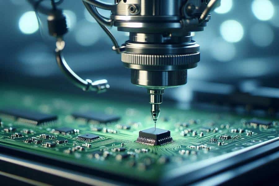
SMT, THT, and mixed technology assembly services, JHYPCB understands that selecting the right soldering chemistry is the foundation of a successful product launch. In this guide, we will break down the technical nuances of compliance and performance to help you determine the optimal path for your specific application.
Navigating the Legal Landscape: RoHS, REACH, and Beyond
In the modern electronics industry, compliance is not an “add-on” feature—it is a mandatory requirement for market entry. The transition from leaded to lead-free soldering was primarily catalyzed by environmental protection and public health initiatives. Understanding these regulations is vital for any OEM looking to distribute products globally.
The RoHS Directive: The Industry Catalyst
The RoHS (Restriction of Hazardous Substances) directive, originated in the European Union and now adopted in various forms globally (such as China RoHS), strictly limits the use of ten hazardous substances, with Lead (Pb) being the most prominent in PCBA.
- The Threshold: For a PCB to be certified as RoHS compliant, the lead content in each homogenous material must be less than 0.1% by weight (1000 ppm).
- The Impact: This regulation effectively banned the traditional Sn63/Pb37 solder for most consumer electronics, necessitating the switch to Lead-Free alloys like SAC305.
REACH Regulation
While RoHS focuses on the final product, REACH (Registration, Evaluation, Authorisation, and Restriction of Chemicals) focuses on the chemical substances used throughout the manufacturing process. As a responsible PCBA partner, JHYPCB ensures that all solder pastes and fluxes used in our SMT lines comply with the latest REACH candidate list of Substances of Very High Concern (SVHC).
The "High-Reliability" Exemptions: Why Leaded Solder Persists
Despite the global push for green electronics, international regulatory bodies recognize that lead-free solder is not yet a “one-size-fits-all” solution. Certain industries are granted exemptions due to the critical nature of their performance and the potential risks of lead-free alternatives (such as tin whiskers).
These exempt sectors often include:
- Aerospace & Defense: Where equipment must withstand extreme vibration and thermal vacuum conditions.
- Medical Devices: Specifically life-support and implantable devices (though many categories are now moving toward mandatory RoHS compliance).
- Automotive (Selected Systems): Particularly in safety-critical sensor systems.
Global Market Variations
It is important to note that compliance requirements vary by region. For instance:
- EU & USA: Strict adherence to RoHS for most commercial goods.
- Specific Industrial Applications: May allow for leaded solder in large-scale stationary industrial tools or high-voltage applications.
JHYPCB Expert Tip: Designing a “Lead-Free” board but using “Leaded” components (or vice-versa) can lead to cross-contamination, which compromises the integrity of the solder joint. Always ensure your Bill of Materials (BOM) aligns with your chosen soldering process.
Technical Performance: Material Characteristics & Reliability
While regulatory compliance dictates the “why,” understanding the physical and chemical differences between leaded and lead-free solder explains the “how.” The transition to lead-free is not a simple substitution; it requires a fundamental shift in the SMT assembly process.
1. The Melting Point Gap
The most immediate difference is the thermal energy required to achieve a reliable solder joint.
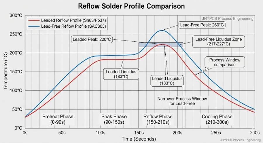
- Leaded Solder (Sn63/Pb37): Features a “Eutectic” melting point of 183°C. This means it transitions from solid to liquid instantly at a relatively low temperature, minimizing thermal stress on sensitive components.
- Lead-Free Solder (SAC305): Requires significantly higher temperatures, typically melting between 217°C and 227°C.
- The Impact: Lead-free SMT assembly necessitates a higher reflow temperature (often peaking at 245°C – 260°C). This creates a narrower “process window” and requires components and PCB substrates (like High-Tg FR4) that can withstand increased thermal shock without delamination or warping.
2. Wetting and Spreading Qualities
“Wetting” refers to the ability of the liquid solder to bond with the copper pads and component leads.
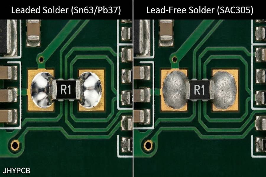
- Superior Wetting (Leaded): Tin-lead solder flows exceptionally well, creating smooth, shiny, and concave solder fillets that are easy to inspect visually.
- Reduced Flow (Lead-Free): Lead-free alloys have higher surface tension. They do not spread as quickly or as widely as leaded solder.
- Visual Difference: Lead-free solder joints often appear “dull” or “grainy” compared to the mirror-like finish of leaded joints. It is crucial for Quality Control (QC) teams to recognize that a dull appearance in lead-free SMT does not necessarily indicate a “cold joint.”
3. Mechanical Reliability and Solder Joint Integrity
How do these joints hold up under real-world stress?
- Ductility: Leaded solder is more “forgiving.” Its ductility allows it to absorb mechanical shocks and thermal expansion stresses effectively.
- Stiffness: Lead-free solder is generally stiffer. While this can provide better fatigue resistance under certain vibration profiles, it can also lead to brittle fractures under extreme mechanical shock.
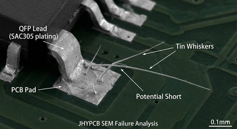
- The “Tin Whisker” Phenomenon: A unique challenge for lead-free (pure tin or high-tin) coatings is the spontaneous growth of microscopic, conductive hair-like structures known as Tin Whiskers. These can cause short circuits in fine-pitch SMT components—a primary reason why the aerospace industry still relies on leaded solder.
4. Comparison Summary Table (For Quick Reference)
| Feature | Leaded Solder (Sn63/Pb37) | Lead-Free Solder (SAC305) |
| Melting Point | 183°C (Low) | 217°C – 227°C (High) |
| Wetting Ability | Excellent | Moderate |
| Joint Appearance | Shiny / Smooth | Dull / Grainy |
| Thermal Stress | Low | High |
| Environmental Impact | High (Toxic) | Low (Eco-friendly) |
| Cost | Lower | Higher (Silver content) |
SMT Manufacturing Process Implications
The shift from leaded to lead-free solder is not merely a change of material; it is a total recalibration of the SMT production line. Higher melting points and different chemical behaviors necessitate precision control over every stage of the assembly process.
1. Reflow Profile Calibration: The 30°C Difference
In lead-free SMT assembly, the “Process Window” becomes significantly narrower. While leaded solder provides a comfortable margin between the melting point (183℃) and the damage threshold of most components, lead-free solder (217℃) pushes the limits.
- Peak Temperature: Lead-free reflow typically peaks at 245°C to 260°C.
- Soak Time: The pre-heat and soak phases must be meticulously managed to ensure uniform heat distribution across the entire PCB, especially for boards with high thermal mass (heavy copper or large BGA components).
- The Risk: If the temperature is too low, you get “cold solder joints”; if it is too high, you risk damaging sensitive ICs, melting plastic connectors, or causing PCB delamination.
2. Component and Substrate Compatibility
Not all components are built for the heat of lead-free assembly. When JHYPCB manages a lead-free project, we perform a rigorous BOM (Bill of Materials) Review to ensure:
- MSL (Moisture Sensitivity Level): Components absorb moisture faster at higher temperatures, increasing the risk of the “popcorn effect” during reflow.
- High-Tg PCB Materials: We often recommend High-Tg (Glass Transition Temperature) substrates (e.g., Tg 170+) for lead-free boards to prevent warping and ensure structural integrity under increased thermal stress.
3. Solder Paste and Flux Chemistry
Because lead-free solder has poorer wetting (flow) characteristics, the Flux chemistry in the solder paste must be more aggressive to remove oxides at higher temperatures.
JHYPCB utilizes advanced No-Clean and Water-Soluble flux systems specifically formulated for SAC305 to ensure that even with reduced wetting, the mechanical bond remains robust and void-free.
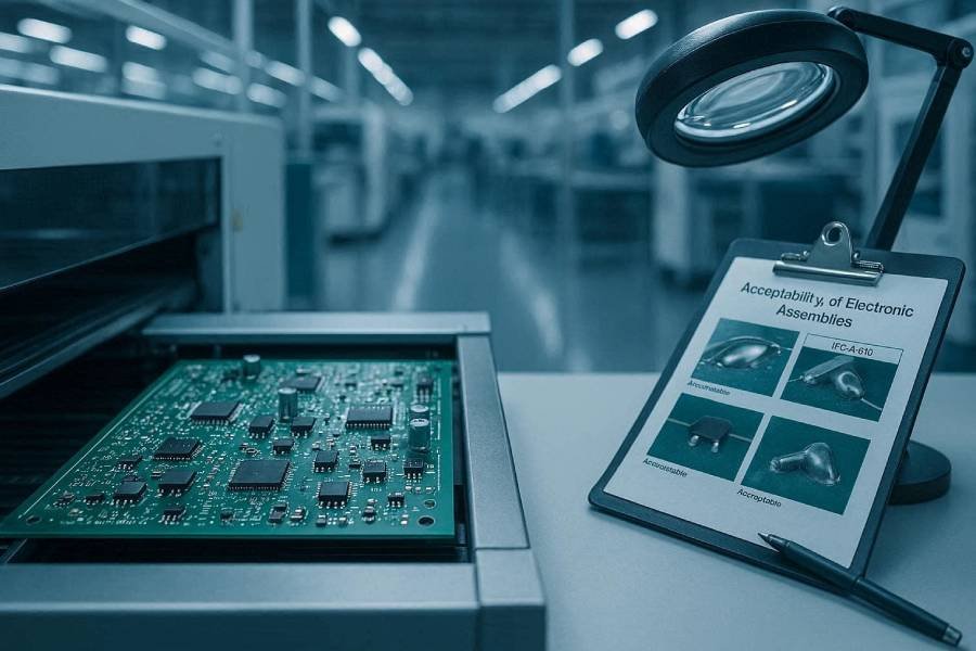
4. Inspection Standards (IPC-A-610)
As mentioned in the previous chapter, lead-free joints look different. This requires specialized training for Quality Assurance (QA) teams.
- Visual Inspection: Inspectors must be trained to IPC-A-610 standards to distinguish between a “dull” lead-free joint (normal) and a “disturbed” or “non-wetting” joint (defect).
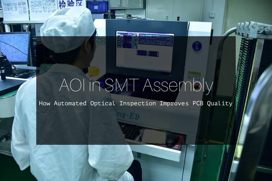
- AOI (Automated Optical Inspection): JHYPCB uses 3D AOI systems with algorithms specifically calibrated for lead-free solder’s light-reflective properties to ensure 100% accuracy in defect detection.
JHYPCB Insight: The move to lead-free requires a “zero-tolerance” approach to moisture. We maintain strict climate-controlled storage and bake components when necessary to eliminate any risk of thermal expansion damage during the 260℃ reflow cycle.
Challenges in Lead-Free SMT Assembly
While the industry has largely standardized lead-free processes, it is not without its technical hurdles. As a high-precision PCBA provider, JHYPCB proactively addresses three primary challenges to ensure the longevity of your hardware.
1. The "Tin Whisker" Phenomenon
Perhaps the most discussed risk in lead-free assembly is the growth of Tin Whiskers. These are microscopic, hair-like crystalline structures that spontaneously grow from surfaces finished with pure tin or high-tin alloys.
The Risk: Because tin whiskers are conductive, they can bridge the gap between fine-pitch SMT pads, leading to intermittent signals or catastrophic short circuits.
The Solution: At JHYPCB, we mitigate this risk by using specific alloy additives (like silver and copper in SAC305), implementing conformal coating when requested, and maintaining strict control over the plating process to minimize internal compressive stress in the solder joints.
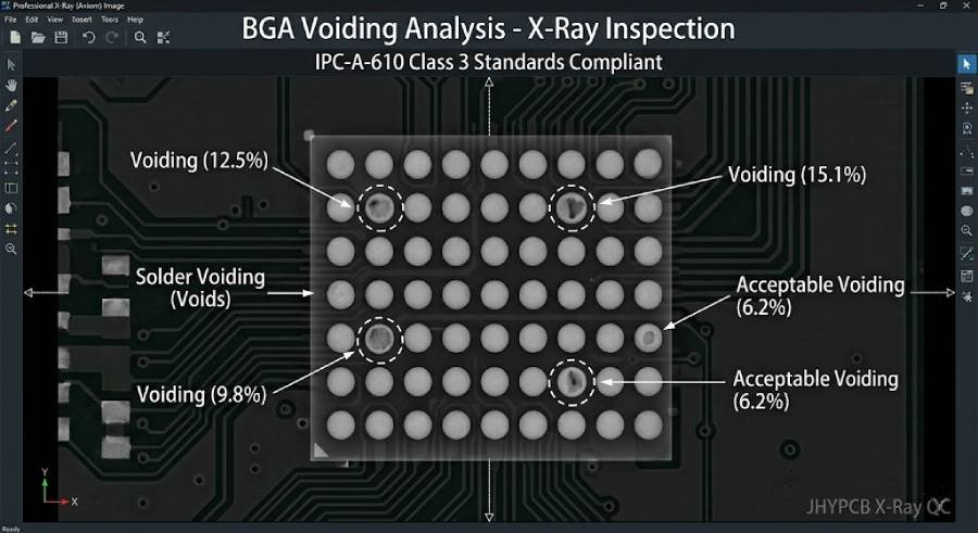
2. Solder Voiding (The "Swiss Cheese" Effect)
Voiding—the formation of small bubbles or gaps within the solder joint—is more prevalent in lead-free processes due to the higher viscosity of the solder and the rapid evaporation of flux at higher reflow temperatures.
The Challenge: Excessive voiding can reduce the thermal and electrical conductivity of the joint and compromise its mechanical strength, especially under BGA (Ball Grid Array) components.
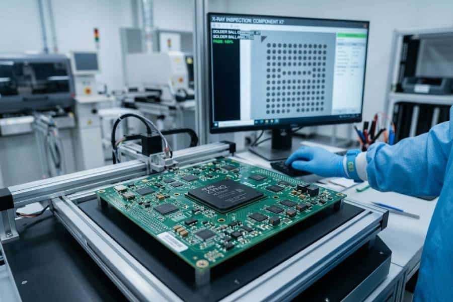
The Solution: We optimize our reflow profiles and use high-grade solder pastes with optimized “out-gassing” properties. Furthermore, we utilize X-Ray Inspection for BGA and QFN components to ensure voiding levels are well within IPC Class 2 or Class 3 limits.
3. Increased Brittleness and Mechanical Stress
Lead-free solder joints are generally stiffer and less ductile than their leaded counterparts.
- The Impact: This stiffness makes the joints more susceptible to cracking when the PCB is subjected to mechanical bending (depaneling), drop tests, or extreme thermal cycling.
- The Solution: JHYPCB employs precision depaneling techniques (such as router-based depaneling instead of manual breaking) to minimize PCB strain. We also advise clients on component placement to avoid putting sensitive parts near high-stress areas of the board.
4. Cost Implications: Materials and Energy
It is no secret that lead-free assembly carries a higher price tag.
- Material Costs: SAC305 contains 3.0% Silver (Ag), making the solder paste significantly more expensive than Sn63/Pb37.
- Energy Consumption: Higher reflow temperatures require more energy and place more wear and tear on the SMT machinery.
- Efficiency: However, by partnering with a high-volume manufacturer like JHYPCB, these costs are offset by our optimized supply chain and high-efficiency production lines.
Leaded Solder: Why It Still Exists
With the global push toward “green” electronics, one might wonder: why has leaded solder not been completely phased out? The answer lies in the uncompromising demands of High-Reliability (Hi-Rel) applications where failure is not an option.
1. The Reliability Factor in Extreme Environments
In certain mission-critical fields, the mechanical and thermal characteristics of Sn63/Pb37 solder provide a level of predictability that lead-free alloys are still struggling to match.
- Superior Ductility: Leaded solder is significantly more flexible than Lead-Free (SAC305). In environments subject to extreme temperature fluctuations (e.g., a satellite orbiting Earth), the solder joints must expand and contract without cracking. The “softness” of lead allows it to absorb this thermal fatigue.
- Vibration Resistance: For aerospace and defense applications, equipment is often subjected to intense G-forces and sustained vibration. Leaded solder joints are less prone to brittle fractures under these conditions.
2. The Tin Whisker Safeguard
As discussed in the previous chapter, Tin Whiskers are a major concern for Lead-Free electronics. In a consumer smartphone, a short circuit might be an inconvenience; in a nuclear power plant control system or a commercial aircraft’s avionics, it could be catastrophic.
- The presence of lead (at least 3%) is the most effective known deterrent to tin whisker growth. For this reason, the Department of Defense (DoD) and NASA often mandate leaded solder for critical systems.
3. Lower Thermal Stress on Legacy Components
Some specialized or “legacy” components are designed with materials that cannot withstand the 260℃ peak temperatures required for Lead-Free reflow.
Leaded soldering(183℃) allows for the assembly of these sensitive parts without risking internal thermal damage, preserving the integrity of the original design.
4. Key Industries Where Leaded Solder Remains the Standard
While JHYPCB is fully equipped for RoHS-compliant production, we continue to support clients in these exempted sectors:
- Aerospace & Aviation: Avionics, flight control systems, and communication satellites.
- Defense & Military: Weapon systems, radar, and ruggedized field equipment.
- Medical Life-Support: Specific implantable devices and diagnostic equipment where long-term stability is proven with leaded alloys.
- Geothermal & Downhole Drilling: Where electronics must operate at high temperatures and high pressures.
Technical Note: When working with leaded solder in a predominantly lead-free world, Prevention of Cross-Contamination is paramount. JHYPCB maintains dedicated soldering stations and strictly separated waste management to ensure that leaded and lead-free processes never interfere with each other.
Choosing the Right Partner for PCBA (The JHYPCB Advantage)
Selecting between leaded and lead-free solder is only half the battle; the other half is choosing an assembly partner capable of executing that choice with zero defects. At JHYPCB, we bridge the gap between complex regulatory requirements and high-performance engineering.
1. Advanced Thermal Management and Reflow Precision
As we’ve discussed, lead-free SMT requires a much higher and tighter temperature window. JHYPCB utilizes multi-zone Lead-Free Reflow Ovens equipped with high-precision thermal sensors. This allows us to create custom reflow profiles for every board, ensuring that even the most heat-sensitive components are protected while achieving perfect solder wetting.
2. Rigorous Quality Inspection (X-Ray & 3D AOI)
Whether you choose the shiny finish of leaded solder or the duller appearance of lead-free, visual inspection is not enough.
- 3D AOI: We use automated optical inspection calibrated for the specific light-reflection properties of lead-free alloys.
- X-Ray Inspection: Essential for BGAs and QFNs, our X-ray systems detect internal voiding and bridging that the naked eye cannot see, ensuring IPC Class 2 or Class 3 compliance.
3. Strict Compliance and Material Traceability
In a global market, “Lead-Free” must be backed by data. JHYPCB provides full material traceability. We ensure that our supply chain is RoHS and REACH compliant, providing you with the necessary documentation to pass environmental audits and clear international customs without delay.
4. Expert DFM (Design for Manufacturing) Support
Our service starts long before the assembly line. During the DFM review, our engineers analyze your BOM and PCB layout to identify potential risks associated with your chosen solder type—such as component temperature ratings or pad designs that might lead to tombstoning in a lead-free environment.
5. Specialized Lines for Leaded & Lead-Free
To serve our clients in the medical, aerospace, and defense sectors, we maintain strict isolation protocols between our leaded and lead-free production areas. This eliminates the risk of cross-contamination, ensuring that your high-reliability boards maintain their intended chemical integrity.
Conclusion
The decision between leaded and lead-free solder in SMT assembly is a balance of regulatory mandate and application-specific reliability. While lead-free is the ethical and legal standard for the vast majority of modern electronics, leaded solder remains a vital tool for the most demanding environments on (and off) the planet.
FAQ: Quick Answers for Engineers
Yes, we offer full-spectrum lead-free services for both surface-mount and through-hole components using wave soldering or selective soldering.
While SAC305 is our standard, we can support other alloys based on specific client requirements for cost or specialized performance.
Through dedicated equipment, separate storage, and rigorous cleaning protocols compliant with international standards.