Table of Contents
In today’s electronics industry, Surface Mount Technology (SMT) has become the backbone of modern PCB assembly. From smartphones and wearables to industrial controllers and automotive systems, the vast majority of electronic products rely on SMT components for compact size, high performance, and cost-effective mass production.
Whether you are a hardware engineer, PCB designer, electronics enthusiast, or procurement specialist, understanding SMT components — their types, package sizes, markings, and manufacturability — is essential for successful product development. Poor component selection or incompatible packaging can lead to assembly defects, increased costs, delayed time-to-market, or even reliability failures.
This comprehensive guide will walk you through everything you need to know about SMT components: from basic concepts to advanced DFM (Design for Manufacturability) considerations. By the end, you’ll be better equipped to make informed decisions that improve assembly yield, reduce costs, and ensure high-quality results.
What Are SMT Components?
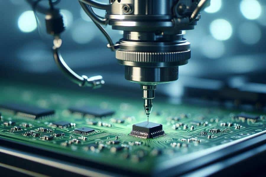
Surface Mount Technology (SMT) components are electronic parts designed to be mounted directly onto the surface of a printed circuit board using automated soldering processes. Unlike traditional through-hole components that require leads to be inserted into drilled holes, SMT components are soldered onto copper pads on the board’s surface. This fundamental difference enables much higher component density and faster, more automated assembly.
SMT vs SMD: Key Differences and Common Confusion
Many people use the terms SMT and SMD interchangeably, but they are not exactly the same:
- SMD (Surface Mount Device) refers to the individual electronic components themselves (resistors, capacitors, ICs, etc.).
- SMT (Surface Mount Technology) refers to the entire assembly process — including solder paste printing, pick-and-place, reflow soldering, and inspection.
In practice, when people say “SMT components,” they usually mean SMDs that are assembled using SMT processes. In this article, we will primarily use “SMT components” as it is the more commonly searched term.
Why SMT Components Are Widely Used in Modern Electronics
SMT components dominate today’s electronics manufacturing for several compelling reasons:
- Miniaturization: SMT packages are significantly smaller than through-hole equivalents, enabling compact, lightweight, and high-density designs.
- Cost Efficiency: Automated assembly is faster and cheaper at scale compared to manual through-hole soldering.
- Better Electrical Performance: Shorter lead lengths reduce parasitic inductance and capacitance, improving signal integrity — especially important for high-frequency and high-speed circuits.
- Higher Production Throughput: Modern pick-and-place machines can place tens of thousands of components per hour.
- Double-sided Assembly: Components can be mounted on both sides of the PCB, maximizing space utilization.
As a result, over 90% of today’s electronic products use SMT as the primary assembly technology.
Where SMT Components Are Used in PCB Assembly
SMT components are used across virtually all electronics sectors:
- Consumer electronics (smartphones, laptops, smartwatches)
- Automotive electronics (ECUs, ADAS systems, infotainment)
- Industrial equipment and IoT devices
- Medical devices and wearables
- Aerospace and high-reliability systems
Understanding the specific requirements of each application is crucial when selecting components and packages.
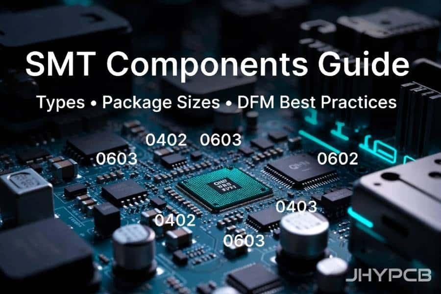
Main Types of SMT Components
SMT components are broadly categorized into passive, active, and other specialized components. Understanding these categories and their characteristics is the first step toward making smart design and procurement decisions.
Passive Components: Resistors, Capacitors, Inductors
Passive components are the most commonly used SMT parts. They do not require external power and typically perform simple functions such as resisting current, storing energy, or filtering signals.
- Resistors The most ubiquitous SMT component. They limit current, divide voltage, and terminate signals. Common types include thick-film and thin-film chip resistors. Available in sizes from 01005 to 2512, with tolerances as tight as 0.1% and power ratings from 0.01W to several watts.
- Capacitors Used for decoupling, filtering, timing, and energy storage. The most popular SMT capacitors are:
- Multilayer Ceramic Chip Capacitors (MLCC) — dominant in most designs
- Tantalum capacitors (for higher capacitance and stability)
- Aluminum electrolytic (larger capacitance, polarized)
- Inductors Used for power filtering, noise suppression, and in DC-DC converters. Common SMT types include wire-wound, multilayer, and molded power inductors. Shielded versions are preferred for high-density boards to reduce electromagnetic interference (EMI).
Tip: When selecting passives, always consider voltage rating, temperature coefficient, and DC bias characteristics (especially important for MLCCs).
Active Components: ICs, Transistors, Diodes, MOSFETs
Active components control the flow of electricity and usually require power to operate. They form the “brain” and “control” sections of a circuit.
- Integrated Circuits (ICs) The most complex SMT components, ranging from simple logic gates to powerful microcontrollers, processors, memory chips, and power management ICs (PMICs). Package choice significantly impacts board density and thermal performance.
- Transistors Primarily Bipolar Junction Transistors (BJT) and Field-Effect Transistors (FETs). Used for switching and amplification.
- Diodes Including rectifier diodes, Schottky diodes, Zener diodes, and Light Emitting Diodes (LEDs — covered separately). They allow current to flow in one direction and are critical for protection, rectification, and signal demodulation.
- MOSFETs The workhorse of modern power electronics. Widely used in power supplies, motor drivers, and battery management systems (BMS) due to their high efficiency and fast switching speeds.
Manufacturing Note: Active components are generally more expensive and sensitive to handling (ESD and MSL — Moisture Sensitivity Level) than passives. Proper storage and baking procedures are often required before assembly.
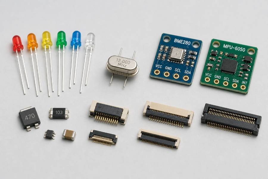
Other Common SMT Components: LEDs, Crystals, Sensors, Connectors, Switches
Beyond traditional passive and active parts, many specialized components are also available in SMT packages:
- LEDs From tiny indicator LEDs to high-power COB and CSP LEDs used in lighting and displays. Polarity and thermal management are critical.
- Crystals and Oscillators Provide precise clock signals for microcontrollers and processors. Common types include quartz crystals, MEMS oscillators, and TCXOs/OCXOs for high-stability applications.
- Sensors Accelerometers, gyroscopes, temperature sensors, pressure sensors, proximity sensors, and environmental sensors (humidity, gas, etc.). Many are now available in ultra-miniature packages for wearables and IoT.
- Connectors Board-to-board, board-to-FPC, and wire-to-board SMT connectors. Mezzanine connectors and high-speed backplane connectors are increasingly common in dense designs.
- Switches and Relays Tactile switches, DIP switches, reed relays, and solid-state relays in SMT form factors.
These “other” components often have unique assembly requirements — such as high coplanarity for connectors or careful reflow profiles for crystals and sensors.
SMT Package Sizes and Codes
One of the most critical decisions in PCB design is choosing the right package size for SMT components. Package size directly affects board space, assembly yield, cost, reliability, and manufacturability. Understanding both imperial and metric coding systems is essential for designers and procurement teams.
Imperial vs Metric Package Codes Explained
SMT chip components (especially passives) use two naming systems:
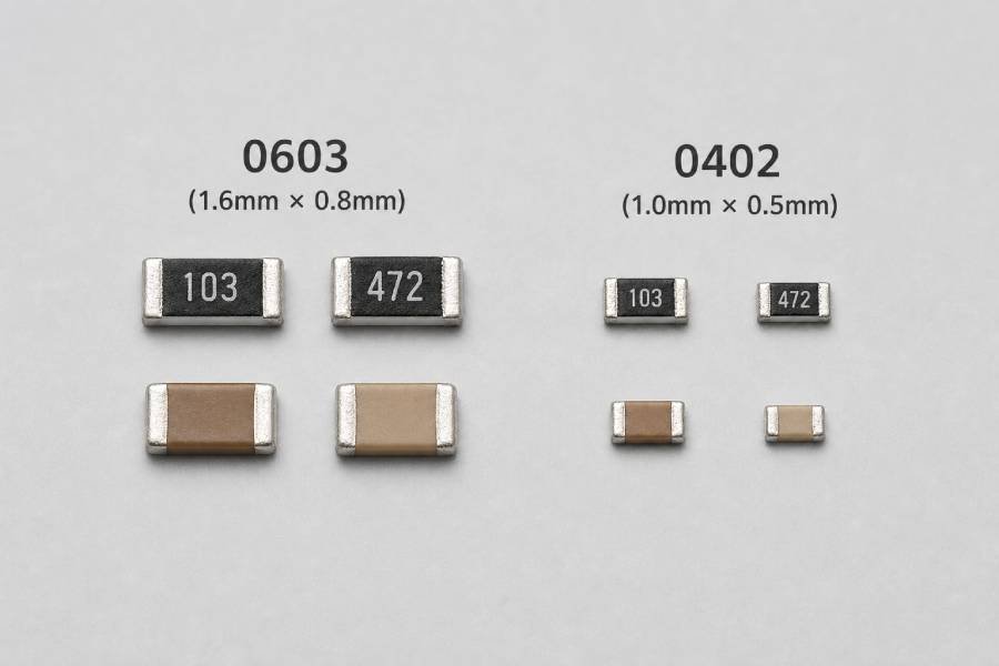
- Imperial Code (most common in datasheets and BOMs): Example: 0402 → 0.04 inch × 0.02 inch (length × width)
- Metric Code (increasingly used by manufacturers): Example: 1005 → 1.0 mm × 0.5 mm
Common Conversion:
| Imperial | Metric | Actual Size (mm) |
|---|---|---|
| 01005 | 0402 | 0.4 × 0.2 |
| 0201 | 0603 | 0.6 × 0.3 |
| 0402 | 1005 | 1.0 × 0.5 |
| 0603 | 1608 | 1.6 × 0.8 |
| 0805 | 2012 | 2.0 × 1.25 |
| 1206 | 3216 | 3.2 × 1.6 |
| 1210 | 3225 | 3.2 × 2.5 |
| 1812 | 4532 | 4.5 × 3.2 |
| 2010 | 5025 | 5.0 × 2.5 |
| 2512 | 6332 | 6.3 × 3.2 |
Pro Tip: Always confirm the actual dimensions in the component datasheet, as some manufacturers may have slight variations.
Popular Sizes: 01005, 0201, 0402, 0603, 0805, 1206 and Larger
Here are the most commonly used sizes in modern electronics:
- 01005 & 0201 Ultra-miniature sizes mainly used in high-density smartphones, wearables, and medical devices. Extremely challenging to assemble.
- 0402 The current mainstream size for consumer electronics. Good balance between density and manufacturability.
- 0603 Very popular for prototypes, hand assembly, and designs where reliability is more important than extreme miniaturization.
- 0805 & 1206 Preferred for higher power applications (resistors, capacitors, inductors) and easier to handle during prototyping and rework.
- Larger sizes (1210 and above) Used for high-power components, connectors, and parts requiring higher mechanical strength.
Package Size Comparison Table
| Package Size | Dimensions (mm) | Typical Power (Resistor) | Typical Capacitance (MLCC) | Assembly Difficulty | Relative Cost | Best Applications |
|---|---|---|---|---|---|---|
| 01005 | 0.4 × 0.2 | 0.03W | Up to 0.1µF | Extremely High | Very High | Smartphones, Ultra-dense boards |
| 0201 | 0.6 × 0.3 | 0.05W | Up to 1µF | Very High | High | Wearables, Mobile devices |
| 0402 | 1.0 × 0.5 | 0.1W | Up to 10µF | High | Medium | Consumer electronics (mainstream) |
| 0603 | 1.6 × 0.8 | 0.1W–0.25W | Up to 47µF | Medium | Low | Prototypes, Industrial |
| 0805 | 2.0 × 1.25 | 0.125W–0.5W | Higher values | Low | Low | Power circuits, Automotive |
| 1206 | 3.2 × 1.6 | Up to 1W | High capacitance | Very Low | Low | High power, LED drivers |
How Package Size Affects Cost, Performance, and Manufacturability
- Smaller Sizes (0201 & 0402): Advantages: Higher component density, smaller PCB size, potentially lower material cost. Disadvantages: Higher component price, significantly more difficult assembly, tighter process control, lower assembly yield, and more challenging rework/repair.
- Larger Sizes (0603 and above): Advantages: Easier and cheaper to assemble, higher yield, better thermal dissipation, easier prototyping and manual rework. Disadvantages: Take up more board space, may increase overall product size and cost.
Key Rule of Thumb: Use the largest package size that your design space and performance requirements allow. This is usually the most cost-effective and reliable approach for production.
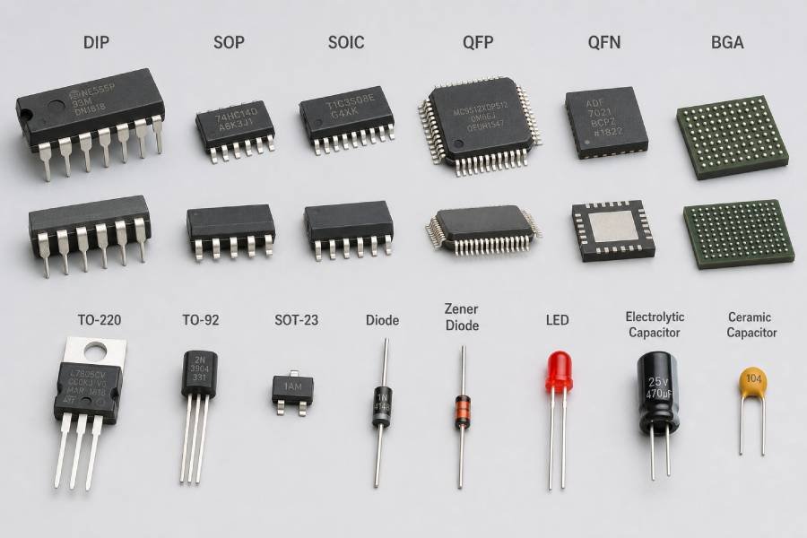
Common SMT Package Types for ICs and Advanced Components
While passive components mostly use simple rectangular chip packages, Integrated Circuits (ICs) and advanced components come in a wide variety of package types. Choosing the right package significantly impacts PCB layout, routing, thermal performance, assembly yield, and long-term reliability.
SOIC, SOP, TSSOP, and Other Gull-Wing Packages
These are traditional gull-wing lead packages, where leads extend outward from the body like wings.
- SOIC (Small Outline Integrated Circuit) One of the most common packages for analog and logic ICs. Wider lead pitch (1.27mm) makes it easier to route and inspect.
- SOP (Small Outline Package) / SSOP (Shrink SOP) Similar to SOIC but with narrower body and lead pitch. TSSOP (Thin Shrink SOP) is even thinner, ideal for space-constrained designs.
- QFP (Quad Flat Package) Leads on all four sides, supporting higher pin counts (up to 256+). eQFP and TQFP (Thin QFP) variants offer better thermal and space performance.
Advantages: Excellent solder joint visibility, easier rework and inspection, forgiving for assembly.
Disadvantages: Larger footprint, lower pin density compared to newer packages.
QFN, DFN, LGA, and BGA Packages
Modern high-density designs have shifted toward leadless and array-style packages:
- QFN (Quad Flat No-lead) / DFN (Dual Flat No-lead) Very popular today. Pads are located under the package body. Excellent thermal performance due to exposed thermal pad.
- LGA (Land Grid Array) Similar to QFN but with a full grid of lands on the bottom. Common in power management and processors.
- BGA (Ball Grid Array) Solder balls arranged in a grid underneath the package. Supports the highest pin counts (hundreds to over 2000). Variants include FBGA, TFBGA, and PoP (Package-on-Package).
Advantages of QFN/LGA/BGA:
- Small footprint and high pin density
- Better electrical performance (shorter connections)
- Superior thermal dissipation (especially with thermal pads)
Disadvantages:
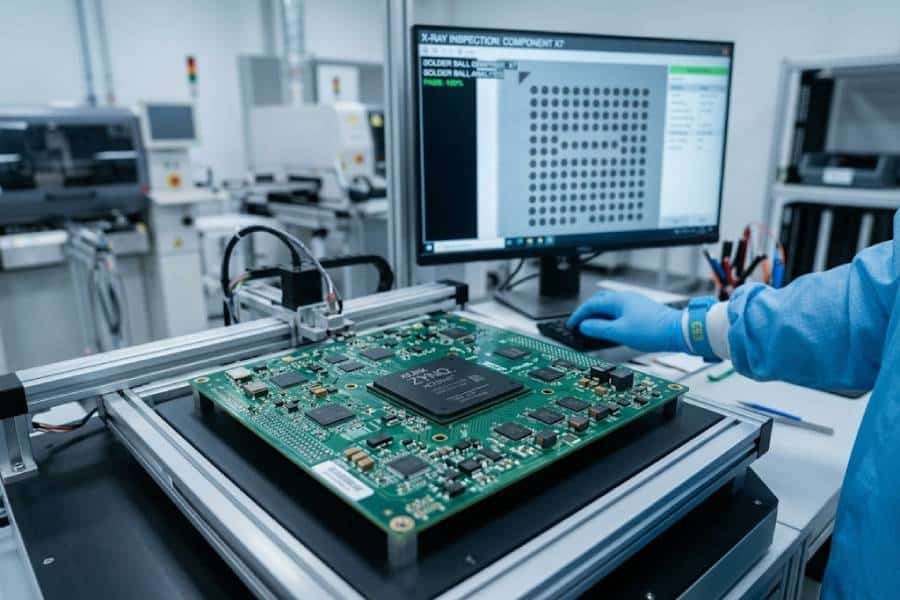
- Hidden solder joints (requires X-ray inspection)
- More difficult rework and debugging
- Higher sensitivity to PCB warpage and coplanarity
Package Selection Criteria: Pin Count, Thermal Management, Board Density, and Routing Feasibility
When choosing between package types, consider the following:
- Pin Count: Use QFP for medium pin counts (up to ~200). Switch to QFN or BGA when pin count exceeds 100–144 for better density.
- Board Density: QFN and BGA allow much tighter component placement than gull-wing packages.
- Routing Feasibility: BGA requires careful via-in-pad or dog-bone routing planning. High-layer count PCBs may be needed for complex BGAs.
- Thermal Requirements: Power ICs (PMICs, motor drivers, CPUs) benefit greatly from QFN/BGA with large thermal pads.
- Cost & Assembly Capability: Gull-wing packages are generally cheaper and easier to assemble. Advanced packages demand better process control and inspection equipment.
Thermal Pad and Exposed Pad Considerations
Most modern QFN, DFN, and some BGA packages feature a large exposed thermal pad (also called EP or DAP) on the bottom.
Key Design Rules:
- The thermal pad must be properly connected to ground planes with multiple thermal vias.
- Via-in-pad design is often required but needs careful solder paste control to avoid voids.
- Adequate solder paste volume and reflow profile are critical to prevent floating or tilting of the package.
- Insufficient thermal relief can lead to overheating and early failure.
Manufacturing Note: Proper thermal pad design is one of the most common causes of field failures in dense designs. Experienced manufacturers can help optimize stencil design and reflow profiles for these packages.
How Component Size and Package Affect SMT Assembly
Component size and package type are among the most important factors influencing SMT assembly success. Choosing an inappropriate size or package can dramatically increase manufacturing difficulty, defect rates, and overall production cost. Understanding these impacts helps designers make better trade-offs between density, performance, and manufacturability.
Placement Accuracy and Pick-and-Place Challenges
Modern pick-and-place machines are highly precise, but component size directly affects placement reliability:
- Ultra-small packages (01005, 0201): Extremely light and tiny, they are prone to being blown away by air currents or misaligned by nozzle vacuum issues. Placement accuracy requirements can reach ±0.05mm or better.
- 0402 and 0603: Mainstream sizes with good balance. Most modern SMT lines handle them reliably at high speed.
- Larger packages (0805+ and high-pin-count ICs): Heavier components require stronger vacuum and slower placement speeds to avoid “tombstoning” or shifting during placement.
BGA and QFN packages add another layer of complexity — they must be placed with high accuracy because their solder joints are hidden underneath, leaving no room for post-placement correction.
Solder Paste Printing and Reflow Sensitivity
Solder paste printing is often the most critical step in SMT assembly, and component size heavily influences it:
- Smaller components (0402 and below): Require very fine pitch stencils (0.1mm or thinner) and high-precision printers. Aperture design becomes extremely sensitive — too much paste causes bridging, too little causes insufficient solder.
- Larger components: More forgiving on paste volume but may need different stencil thicknesses or stepped stencils when mixed with small components on the same board.
- Packages with thermal pads (QFN, BGA): Demand carefully calculated paste volume to avoid solder voids or package floating during reflow.
Reflow soldering profiles must also be adjusted according to package size and thermal mass. Small components heat up faster, while large BGAs or power inductors require more heat, increasing the risk of overheating nearby small parts.
Why Smaller Packages Require Stronger Process Control
As package sizes shrink, the process window narrows significantly:
- Higher sensitivity to PCB warpage, temperature variations, and material quality.
- Increased risk of defects such as tombstoning, billboarding, skewing, and solder bridging.
- More stringent requirements for stencil cleaning frequency, solder paste type (Type 4 or Type 5), and environmental control (humidity and temperature).
- Tighter coplanarity and pad flatness requirements on the PCB.
Industry Rule of Thumb: For designs using 0201 or 01005 components, the SMT assembly house should have advanced equipment (such as high-resolution 3D SPI — Solder Paste Inspection, and 3D AOI) and experienced process engineers. Not all manufacturers can reliably handle high volumes of ultra-small components.
Common Assembly Defects Related to Component Selection
Poor component size or package choices frequently lead to the following defects:
- Tombstoning: One end of a small resistor or capacitor lifts up during reflow.
- Bridging and Shorts: Common with fine-pitch QFN, DFN, and 0201/0402 components.
- Insufficient Solder / Open Joints: Especially on BGA and QFN thermal pads.
- Component Rotation or Skew: Frequent with very small or asymmetric packages.
- Head-in-Pillow (HiP): A common defect in large BGA packages due to improper reflow profiling.
Early DFM analysis and proper component selection can prevent most of these issues before production begins.
How to Choose the Right SMT Components for Your Design
Selecting the right SMT components is both a technical and strategic decision. A good choice balances electrical performance, physical constraints, cost, availability, and manufacturability. Poor decisions at this stage often lead to redesigns, supply chain delays, or production yield issues.
Balancing Performance, Cost, Size, and Availability
When choosing components, consider these four key factors together:
- Performance: Ensure the component meets your electrical requirements (tolerance, voltage rating, frequency response, power handling, etc.). For example, select X7R or X5R MLCCs for most decoupling applications, but use C0G/NP0 for precision timing circuits.
- Size: Smaller packages (0402 and below) save board space but increase assembly cost and risk. Larger packages (0603/0805) improve manufacturability and reliability.
- Cost: Unit price matters, but total cost of ownership (including assembly yield, sourcing effort, and potential rework) is more important. Sometimes a slightly more expensive component saves money overall.
- Availability: Check stock across multiple distributors (Digi-Key, Mouser, LCSC, etc.) early in the design phase. Long lead times on specialized parts can delay your entire project.
Practical Tip: Create a component selection scorecard that assigns weights to each factor based on your project priorities (e.g., prototype vs mass production).
Reliability, Power Handling, and Environmental Requirements
- Reliability: For industrial, automotive, or medical applications, choose components with higher temperature ratings (125°C or 150°C), automotive-grade (AEC-Q200), or extended lifetime specifications.
- Power Handling: Always derate components. For resistors, use no more than 50% of rated power in high-ambient-temperature environments. For capacitors, pay attention to DC bias derating on MLCCs.
- Environmental Factors: Consider operating temperature range, humidity, vibration, and exposure to chemicals. Select components with appropriate MSL (Moisture Sensitivity Level) ratings and conformal coating compatibility when needed.
High-reliability designs should prioritize components from established manufacturers with strong quality systems.
Sourcing Best Practices: Second Sourcing, Obsolescence, and Counterfeit Prevention
- Second Sourcing: Identify at least one (preferably two) alternative manufacturers for critical components. Ensure pin-to-pin and footprint compatibility.
- Obsolescence Management: Use tools like SiliconExpert or Octopart to check product lifecycle status. Avoid components that are already “Not Recommended for New Designs” (NRND).
- Counterfeit Prevention:
- Purchase only from authorized distributors
- Request original manufacturer certificates of conformance (CoC)
- For high-risk parts, consider third-party testing or X-ray inspection upon receipt
JHYPCB’s procurement team regularly helps customers identify reliable alternatives and mitigate sourcing risks during BOM review.
BOM Optimization Tips Before Production
- Standardize component values and packages across the design (e.g., use as few different resistor values as possible).
- Prefer components that are already in the assembly house’s preferred vendor list (this reduces setup costs and lead times).
- Group similar packages together on the PCB to optimize pick-and-place efficiency.
- Perform a thorough BOM scrub: remove obsolete parts, combine similar items, and flag high-risk components.
- Consider “Common Parts” strategy — using popular, high-volume parts (e.g., common 0402 resistors) dramatically improves availability and lowers cost.
Golden Rule: Finalize your BOM only after a professional DFM and DFA (Design for Assembly) review.
SMT Component Markings, Polarity, and Identification
Accurate identification of SMT components is crucial for design verification, incoming quality control, assembly programming, and troubleshooting. Misreading markings or ignoring polarity can lead to costly assembly errors, debug nightmares, or field failures.
How to Read Markings on Resistors, Capacitors, and ICs
Resistors Most chip resistors use numeric coding:
- 3-Digit Code (common in 5% tolerance): e.g., 103 = 10 × 10³ Ω = 10kΩ
- 4-Digit Code (1% tolerance): e.g., 1002 = 100 × 10² Ω = 10kΩ
- EIA-96 Code (high precision): Uses two digits + one letter (e.g., 01A = 100Ω)
Zero-ohm resistors are marked as 000 or a single 0.
Capacitors (MLCC) Markings are less standardized:
- Many small MLCCs (0402 and below) have no markings due to limited space.
- Larger ones may show capacitance code (e.g., 106 = 10µF) and voltage rating.
- Tantalum capacitors usually show capacitance, voltage, and polarity.
Integrated Circuits (ICs) IC markings typically include:
- Manufacturer logo or prefix
- Part number (e.g., SN74LVC245 or STM32F103)
- Date code (e.g., YYWW = Year + Week)
- Lot number and revision code
Tip: Always cross-reference the marking with the official datasheet. Tools like Octopart or component search engines can help decode markings quickly.
Polarity Indicators and Orientation Best Practices
Many SMT components are polarized and must be placed in the correct orientation:
- Diodes and LEDs: Cathode is usually marked with a line, dot, or chamfer on the package.
- Tantalum and Electrolytic Capacitors: Positive terminal is often marked with a line or bar (note: conventions vary by manufacturer).
- ICs:
- Pin 1 indicator: Dot, notch, chamfered corner, or beveled edge.
- QFN/BGA: Usually have a small dot or marking in corner for Pin 1.
- Crystals and Oscillators: Some have a clear polarity or ground pin marking.
Design Best Practices:
- Clearly indicate polarity and Pin 1 in your PCB footprint and silkscreen.
- Use asymmetric pad shapes or courtyard markings for polarized components.
- In CAD libraries, enable polarity indicators and rotation locks where possible.
- During assembly, provide clear orientation documentation (especially for manual prototypes).
Common Identification Mistakes and How to Avoid Them
- Reading old markings on reels: Tape-and-reel labels can be misread — always verify the component itself when in doubt.
- Confusing similar-looking packages: 0402 resistors and capacitors look nearly identical without magnification.
- Polarity reversal: Extremely common with diodes, LEDs, and tantalum caps. Can cause immediate damage.
- Date code confusion: Mistaking date codes for part values.
- Counterfeit parts: Fake components often have poor or incorrect laser markings.
Prevention Strategies:
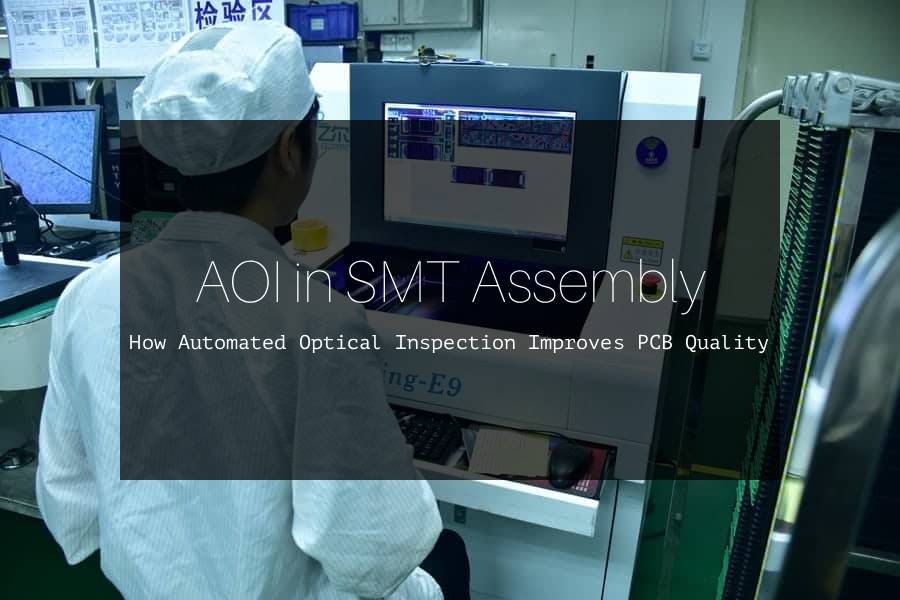
- Use automated optical inspection (AOI) during assembly.
- Request component datasheets and marking specifications in your BOM.
- Perform sample incoming inspection with a microscope or video inspection system.
- Work with experienced assembly partners who maintain strict component verification processes.
Proper marking identification and polarity management significantly reduce assembly defects and speed up debugging.
DFM Considerations for SMT Components
Design for Manufacturability (DFM) is where theoretical design meets real-world production. Even the best component selection can fail if DFM rules are ignored. Proper DFM for SMT components significantly improves assembly yield, reduces defects, and lowers overall production costs.
Footprint and Pad Design Guidelines
Accurate footprints are the foundation of reliable SMT assembly:
- Follow IPC-7351 standards for land patterns (most CAD libraries comply, but always verify).
- For chip components (resistors/capacitors): Use recommended pad sizes with proper solder mask expansion (NSMD — Non-Solder Mask Defined is usually preferred for small packages).
- For QFN and BGA: Pay special attention to thermal pad design, including via placement, via tenting or filling, and solder mask defined (SMD) vs non-solder mask defined pads.
- Ensure pad-to-trace connections have proper thermal relief where needed, but avoid excessive relief on high-speed or power signals.
Common Mistake: Using generic library footprints without customization for your specific PCB stack-up and assembly process.
Component Spacing, Orientation, and Keep-Out Zones
Proper spacing prevents assembly and reliability issues:
- Minimum Spacing: Maintain at least 0.3–0.5mm between 0402 components, and more for larger packages. Follow your assembly partner’s DFM guidelines.
- Orientation Best Practices:
- Align similar components in the same rotation direction to optimize pick-and-place speed.
- Avoid placing small components too close to large thermal-mass parts (can cause uneven heating during reflow).
- Keep-Out Zones: Reserve adequate space around BGAs, connectors, and high-power components for inspection, rework, and heat dissipation.
- Keep sensitive components (crystals, sensors, RF modules) away from noisy switching regulators.
Stencil Design and Solder Joint Reliability
Stencil design is critical for solder paste deposition:
- Aperture Design: Use 1:1 ratio for most 0603+ components. For 0402 and smaller, reduce aperture area by 5–15% to prevent bridging.
- Stencil Thickness: 0.1mm (4 mil) is standard for mixed assemblies; 0.08mm or 0.127mm for ultra-fine pitch.
- Thermal Pads: Use home-base or window-pane aperture patterns to control paste volume and reduce voids.
- Via-in-Pad: Require filled or tented vias to prevent solder wicking.
Good stencil design directly improves solder joint quality and reduces defects like head-in-pillow, insufficient solder, and bridging.
Moisture Sensitivity (MSL) and Handling Requirements
Many active components (especially QFN, BGA, and some LEDs) are moisture-sensitive:
- Check the MSL rating (Level 1 to 6) in the datasheet. MSL 3 and above usually require baking before assembly if the floor life is exceeded.
- Store components in dry boxes with desiccant and humidity indicators.
- High-MS L parts need strict control of exposure time between removal from moisture barrier bags and reflow.
Failure to manage MSL properly can cause “popcorning” (internal package cracking during reflow), leading to early field failures.
DFM Checklist for SMT Component Selection
Use this checklist before releasing your design for production:
- All footprints match manufacturer recommended land patterns
- Component spacing meets minimum DFM rules
- Polarized components have clear silkscreen orientation marks
- High-pin-count packages (QFN/BGA) have proper thermal via arrays
- Mixed package sizes are grouped logically when possible
- Critical components have second sources with compatible footprints
- MSL-rated parts are clearly flagged in the BOM
- Stencil and paste considerations reviewed for fine-pitch devices
Pro Tip: Always submit your Gerber files, BOM, and pick-and-place files for a professional DFM review before ordering. Early feedback can save weeks of redesign.
At JHYPCB, our engineering team performs free DFM analysis for all turnkey SMT assembly orders, helping customers catch issues before production begins.
SMT Components in Different Applications
The optimal choice of SMT components varies significantly depending on the end application. Factors such as size constraints, reliability requirements, operating environment, cost sensitivity, and production volume all influence component and package selection.
Consumer Electronics and Wearables
Consumer products like smartphones, smartwatches, true wireless earbuds (TWS), and tablets prioritize extreme miniaturization and high component density.
- Dominant package sizes: 01005, 0201, and 0402
- Heavy use of advanced packages: CSP (Chip Scale Package), WLCSP, PoP (Package-on-Package), and ultra-thin QFN
- Key component characteristics: Low profile, high capacitance in small packages (MLCCs), and excellent power efficiency
- Challenges: Very tight process control, high placement accuracy, and strict thermal management in compact enclosures
In this segment, cost pressure is high and time-to-market is critical. Manufacturers often need advanced SMT lines capable of handling large numbers of tiny components with high yield.
Industrial, Automotive, and Medical Electronics
These applications demand significantly higher reliability and robustness compared to consumer electronics.
- Automotive Electronics (ECUs, ADAS, BMS, infotainment):
- Prefer 0603 to 1206 packages for better reliability
- AEC-Q200 qualified components
- Wider temperature range (-40°C to +125°C or +150°C)
- Enhanced vibration and thermal cycling resistance
- Industrial Equipment & IoT: Mix of 0402/0603 for density and larger packages for power circuits. Long-term availability and stable supply chains are crucial.
- Medical Devices: High reliability, low failure rates, and often biocompatibility or sterilization compatibility. Components must support long service life with strict traceability.
Common requirements across these sectors include better derating, redundant designs for critical circuits, and thorough DFM validation.
High-Density, High-Frequency, and High-Reliability Designs
Specialized applications such as 5G infrastructure, RF modules, servers, aerospace, and defense push SMT technology to its limits:
- High-Density: Extensive use of BGA, LGA, and fine-pitch QFN with micro-vias and HDI PCBs
- High-Frequency / RF:
- Low-tolerance components (0.1% resistors, C0G capacitors)
- Shielded inductors and high-Q components
- Careful attention to parasitic inductance and controlled impedance routing
- High-Reliability:
- Ceramic capacitors instead of tantalum where possible
- High-temperature-rated components
- Enhanced inspection (X-ray, 3D AOI, Flying Probe testing)
These designs typically require close collaboration between designer and assembly partner to optimize component selection, PCB stack-up, and process parameters.
Key Takeaway: Always match your SMT component strategy to the actual application requirements. A component choice that works perfectly for a consumer product may fail in an automotive or medical environment — and vice versa.
Frequently Asked Questions (FAQ)
Here are answers to the most common questions about SMT components that engineers, designers, and procurement teams frequently ask.
No, they are related but not identical. SMD (Surface Mount Device) refers to the components themselves — resistors, capacitors, ICs, etc. designed for surface mounting. SMT (Surface Mount Technology) refers to the assembly process used to mount those components onto a PCB.
In everyday conversation, people often say “SMT components” to mean SMDs assembled via SMT. The terms are frequently used interchangeably, but technically they describe different aspects.
For beginners and early prototyping, 0603 or 0805 are the most recommended sizes.
Reasons:
- Easier to handle manually
- More forgiving during soldering (hand soldering or hot air rework)
- Lower risk of assembly defects
- Widely available and inexpensive
Once your design is proven and you move to production, you can consider migrating to 0402 for higher density if needed. Avoid starting with 0201 or 01005 unless your project specifically requires ultra-miniaturization.
Yes, BGA (Ball Grid Array) is considered an SMT component.
BGA packages are mounted directly onto the surface of the PCB using solder balls, as part of the SMT assembly process. They are one of the most advanced SMT package types and are widely used in high-density designs such as processors, memory chips, and power management modules. Because their solder joints are hidden, they require X-ray inspection during quality control.
| Aspect | 0402 | 0603 |
|---|---|---|
| Dimensions | 1.0 × 0.5 mm | 1.6 × 0.8 mm |
| Typical Power Rating | 0.1W | 0.1W ~ 0.25W |
| Assembly Difficulty | High | Medium |
| Placement Accuracy | Tighter tolerance | More forgiving |
| Best For | High-density consumer electronics | Prototypes, industrial, general use |
| Relative Cost | Higher | Lower |
0402 offers better space saving but is more challenging to assemble reliably. 0603 provides a better balance of manufacturability and reliability for most applications.
It depends on your manufacturer’s capabilities.
- 0603 and above: Reliable for almost all standard SMT assembly houses.
- 0402: Reliable for most professional manufacturers with modern equipment.
- 0201: Requires advanced SMT lines and experienced process control. Yield drops if the manufacturer lacks fine-pitch capability.
- 01005: Only recommended for companies with high-end equipment and proven track records in ultra-high-density assembly. Not suitable for most prototype or low-to-medium volume production.
Recommendation: Always discuss your smallest package size with your PCB assembly partner during the DFM review stage. They can tell you exactly what is feasible within your budget and timeline.
- Should I use the same package size for all passive components? Ideally yes — standardizing sizes improves assembly efficiency and reduces errors.
- Do all SMT components need moisture sensitivity control? Only MSL-rated components (mostly ICs, BGAs, QFNs). Most passive components are MSL 1 and not sensitive.
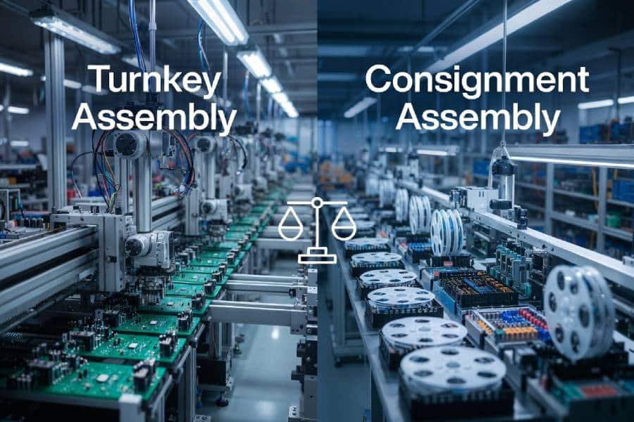
Why Smart SMT Component Selection Matters for Turnkey PCB Assembly
In a turnkey PCB assembly project, where one supplier handles component sourcing, PCB fabrication, SMT assembly, and testing, component selection decisions have an outsized impact on the entire project outcome. A well-optimized BOM can save weeks of lead time, reduce costs by 10–30%, and dramatically improve final product quality.
Impact on Sourcing Lead Time and Cost
Component selection directly influences procurement efficiency:
- Availability: Popular, high-volume components (common 0402 resistors, 0603 capacitors, mainstream MCUs) are usually in stock with short lead times. Rare or obsolete parts can extend lead time from days to months.
- Cost Structure: Using non-standard or low-volume packages increases unit price and may incur high minimum order quantities (MOQ). Standardizing components across the BOM reduces overall material cost.
- Multi-Sourcing Risk: Smart selection includes identifying second sources early, avoiding single-source bottlenecks during global supply chain disruptions.
In turnkey projects, experienced assemblers like JHYPCB maintain deep relationships with major distributors and factories, giving them better access and pricing — but only when the BOM is optimized.
Impact on Assembly Yield, Quality, and Reliability
Component choice significantly affects production success:
- Assembly Yield: Smaller packages (0201/0402) and complex packages (fine-pitch QFN, high-ball BGA) require tighter process control. Poor choices can drop first-pass yield from 99%+ to below 95%, increasing rework and scrap costs.
- Quality & Defects: Incompatible thermal masses, improper polarity handling, or unsuitable MSL-rated parts lead to common defects like tombstoning, voids, bridging, and popcorning.
- Long-term Reliability: Using under-rated components, ignoring temperature derating, or selecting packages with poor thermal performance can cause field failures months or years later.
A professional turnkey partner will catch many of these issues during DFM review, but starting with a manufacturable BOM makes the entire process smoother and more cost-effective.
How JHYPCB Helps Optimize Your BOM and SMT Process
At JHYPCB, we don’t just assemble boards — we help customers make smarter component decisions:
- Free BOM Analysis & Optimization: We review your BOM for availability, cost reduction opportunities, second-source suggestions, and obsolescence risks.
- DFM/DFA Review: Detailed feedback on package sizes, footprints, spacing, stencil design, and process capability.
- Preferred Component Library: Access to components we regularly stock or source at competitive prices with proven assembly performance.
- Full Turnkey Support: From component sourcing and PCB fabrication to SMT/THT/mixed assembly, functional testing, and final packaging — all under one roof with strict quality control.
Many customers have reduced their total project cost by 15–25% and shortened lead times simply by implementing our BOM optimization recommendations.
Bottom Line: Smart SMT component selection is one of the highest-ROI decisions you can make in electronics development. It affects not only your board performance but also your project timeline, budget, and product reliability.
Partner with JHYPCB for Your SMT PCB Assembly Needs
Choosing the right manufacturing partner is just as important as selecting the right SMT components. With over a decade of experience in PCB fabrication and assembly, JHYPCB has helped thousands of engineers and companies worldwide bring their designs from prototype to mass production successfully.
Full Turnkey SMT, THT, and Mixed Assembly Services
We offer comprehensive turnkey PCB assembly solutions, including:
- SMT Assembly (supporting 01005 to large BGAs)
- THT (Through-Hole Technology) Assembly
- Mixed Technology Assembly
- Component sourcing from reliable global suppliers
- PCB fabrication (1–40 layers, including HDI)
- Conformal coating, potting, and final product assembly
Our one-stop service eliminates the hassle of coordinating multiple suppliers, reduces communication overhead, and ensures better quality consistency.
Rapid Prototyping and Volume Production Capabilities
Whether you need 5 pieces for prototyping or 50,000+ units for mass production, JHYPCB has you covered:
- Quick-turn Prototyping: 24–48 hour turnaround available for urgent projects
- Flexible Production: Seamless scaling from NPI (New Product Introduction) to volume manufacturing
- Advanced SMT Lines: High-speed placement systems capable of handling ultra-fine pitch components, complex BGAs, and high-density designs with excellent yield
Free DFM Review, BOM Analysis, and Expert Support
Our biggest advantage is our engineering-first approach:
- Free DFM/DFA Analysis before production
- BOM Optimization with cost reduction and availability suggestions
- Expert Component Recommendations based on your specific application and volume
- Dedicated project engineers to support you throughout the entire process
- Rigorous quality control including SPI, 3D AOI, X-ray, ICT, and functional testing
We specialize in helping customers solve complex SMT challenges — from ultra-miniature wearable devices to high-reliability automotive and industrial electronics.
Get a Quote for Your Next SMT Project
Ready to move forward with your project?
Upload your Gerber files, BOM, and assembly drawings today and receive a competitive quote within hours. Our team will also provide a free DFM report and component optimization suggestions to help you reduce cost and improve manufacturability.
Contact JHYPCB today for reliable, high-quality SMT PCB assembly services backed by professional engineering support and fast turnaround.