


4 Layer PCB Manufacturing & Prototype Service
Factory‑direct 4 layer PCB with standard FR4 stackup, fast prototype lead time, and free DFM support.
We specialize in manufacturing standard and custom 4 layer PCBs with optimized stackup for signal integrity and EMI performance, from quick-turn prototypes to volume production.
With in‑house multilayer PCB fabrication, we offer cost‑effective 4 layer PCB pricing, fast turnaround, and one‑on‑one engineering review to ensure your design is manufacturable before production.
- Fast 4 layer PCB prototype and production lead time.
- Competitive global pricing with flexible low‑volume and bulk orders.
- Free DFM check and engineering support before manufacturing.
Trusted 4 layer PCB manufacturer for communication, industrial control, IoT, and consumer electronics projects worldwide.
What Is a 4 Layer PCB?
A 4 layer PCB (four‑layer printed circuit board) is a multilayer circuit board that contains four copper layers laminated together with insulating dielectric material, typically FR4.
Compared with a simple 2 layer PCB, a 4 layer board adds internal power and ground planes, which improves signal integrity, EMI performance, and power distribution in compact designs.

4 Layer PCB Structure and Layer Functions
In a standard 4 layer PCB structure, the two outer layers (top and bottom) are mainly used for component placement and signal routing, just like a 2 layer PCB.
The two inner layers typically act as solid planes – one for ground (GND) and one for power (VCC) – providing low‑impedance return paths for high‑speed signals and helping to reduce electromagnetic interference (EMI).
This 4 layer PCB stackup offers more routing channels and better reference planes than a 2 layer PCB, while staying more cost‑effective and easier to manufacture than a 6 layer or 8 layer board.
For many modern products, this balance of performance, board size, and cost makes a standard 4 layer circuit board the preferred choice over both basic double‑sided and very high‑layer‑count PCBs.
As a result, 4 layer PCBs are widely used in communication devices, industrial controllers, consumer electronics, IoT products, and other designs that require stable power delivery, clean high‑speed signals, and compact layouts.
Standard 4 Layer PCB Stackup & Thickness
A standard 4 layer PCB stackup arranges the copper and dielectric layers in a way that balances signal integrity, EMI performance, manufacturability, and cost.
The most common 4 layer FR4 PCB stackup uses the outer layers for signal routing and the inner layers as solid power and ground planes, creating stable reference planes for high‑speed designs.
Typical 4 Layer FR4 PCB Stackup
One typical 4 layer PCB stackup for general‑purpose designs is: Top signal layer, Inner ground plane, Inner power plane, and Bottom signal layer.
This signal–ground–power–signal configuration provides tight coupling between the planes, short return paths for signals, and good shielding, which helps control impedance and reduce crosstalk in many 4 layer circuit boards.
| Layer | Function | Notes |
|---|---|---|
| Top layer | Signal + components | Main routing layer for critical signals |
| Inner layer 1 | Ground plane (GND) | Solid reference plane for return currents |
| Inner layer 2 | Power plane (VCC) | Stable power distribution for devices |
| Bottom layer | Signal + components | Secondary routing and I/O connections |

Standard & Typical 4 Layer PCB Stackup
4 Layer PCB Thickness and Dielectric Options
The standard 4 layer PCB thickness is typically around 1.6 mm (about 0.063 inch), but common options range from about 0.8 mm to 2.4 mm depending on design requirements. By adjusting core and prepreg dielectric thickness between layers, we can support typical 4 layer PCB thickness values such as 0.8 mm, 1.0 mm, 1.2 mm, and 1.6 mm while maintaining controlled impedance for high‑speed signals.
For most standard FR4 4 layer PCBs, outer copper thickness typically starts from 1 oz, with options for thicker copper when higher current or better thermal performance is required. Thinner 4 layer boards around 0.8 mm are often used in compact consumer and IoT products, while 1.6 mm boards are common in industrial controllers and general‑purpose electronics where mechanical strength is important.
1. First Type of 4 Layer PCB Stackup and Layout
- Stackup: Top Layer – Signal, Inner Layer 1 – Power, Inner Layer 2 – Ground, Bottom Layer – Signal
- Layout Tips: Place signal traces on the outer layers for easy access. Ensure the power and ground planes are closely spaced to minimize impedance and enhance EMI shielding.
- Best For: General-purpose designs requiring balanced signal routing and power distribution.
The close proximity of power and ground layers improves decoupling, but a thicker core or prepreg may require careful impedance matching.
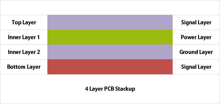
The first type of 4 layer PCB stack up
2. Second Type of 4 Layer PCB Stackup and Layout
- Stackup: Top Layer – Power, Inner Layer 1 – Signal, Inner Layer 2 – Signal, Bottom Layer – Ground
- Layout Tips: Route high-speed signals on inner layers to reduce EMI. Use the top power layer for decoupling capacitors and the bottom ground layer as a reference plane.
- Best For: High-speed applications where shielding and signal integrity are critical.
This setup offers robust EMI protection due to the shielding effect of power and ground planes, though component placement near the edges requires attention.
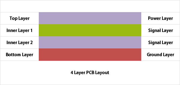
The second type of 4 layer PCB stack up
3. Third Type of 4 Layer PCB Stackup and Layout
- Stackup: Top Layer – Signal, Inner Layer 1 – Ground, Inner Layer 2 – Power, Bottom Layer – Signal
- Layout Tips: Prioritize ground plane proximity to signal layers for better noise reduction. Route power planes to avoid interference with high-density components.
- Best For: Complex designs with high component density and stringent grounding needs.
This configuration enhances signal quality but may limit top-layer accessibility, requiring optimized via placement.
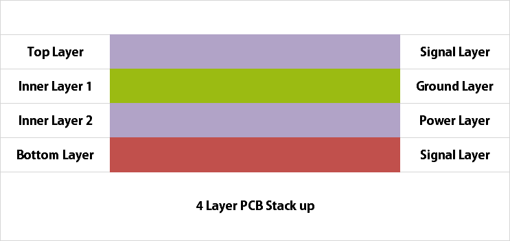
The third type of 4 layer PCB stack up
Choosing the right stackup and layout depends on your project’s specifications, such as signal speed and EMI tolerance. JHYPCB offers tailored 4-layer PCB design and prototyping services to ensure your layout meets industry standards.
For more layout tips and stackup examples, download our comprehensive guide: Click here for the 4-16 Layer PCB Stackup and Layout Guide.
Need help with 4-layer PCB design? Download our free tutorials for popular PCB design software to get started:
4 Layer PCB Capabilities & Specifications
Our 4 layer PCB capabilities cover standard FR4 boards as well as higher‑performance materials for RF, high‑speed, and special applications. With flexible options in board thickness, copper weight, minimum trace/space, and drill sizes, we support both cost‑effective prototypes and demanding production‑grade 4 layer circuit boards.
Standard FR4 4 Layer PCB Capabilities
The table below shows our typical manufacturing capabilities for standard FR4 4 layer PCBs.
| Specification | Typical Capability (4 layer FR4 PCB) |
|---|---|
| Board material | Standard FR4 (TG options available) |
| Layer count | 4 layers multilayer PCB |
| Standard board thickness | 1.6 mm (other options: 0.8 / 1.0 / 1.2 mm) |
| Copper thickness | 1 oz outer layers (0.5–2 oz options) |
| Min trace/space | e.g. 4/4 mil or better depending on stackup |
| Min finished hole size | e.g. 0.2–0.25 mm mechanical drill |
| Surface finishes | HASL, lead‑free HASL, ENIG, others on request |
| Solder mask colors | Green (standard), black, white, red, blue, etc. |
| Silkscreen colors | White, black (depending on solder mask) |
| Testing | 100% electrical test for 4 layer PCB production |
Advanced 4 Layer PCB Options
In addition to standard FR4 4 layer PCBs, we also support advanced materials and stackups for higher‑performance designs. For RF and high‑frequency applications, we can combine FR4 with low‑loss laminates to build 4 layer RF PCBs and 4 layer Rogers boards with controlled impedance and tighter loss budgets.
For space‑constrained products, we manufacture 4 layer rigid‑flex PCBs that combine rigid and flexible sections in one structure. By properly designing the rigid‑flex stackup and bend radius, we help reduce connectors, improve reliability, and simplify assembly.
4 Layer Rigid‑Flex and Special Requirements
For space‑constrained products, we can manufacture 4 layer rigid‑flex PCBs that combine rigid and flexible sections into one connected structure.
By carefully designing the 4 layer rigid‑flex PCB stackup and bend radius, we help you reduce connectors, improve reliability, and simplify assembly in complex devices.
Whether you need a cost‑effective standard 4 layer FR4 PCB, a high‑performance 4 layer RF PCB, or a customized 4 layer stackup, our engineering team can review your requirements and recommend suitable specifications before manufacturing.
Not sure if your 4 layer PCB design fits these limits? Upload your Gerber files for a free DFM check and capability review.
Applications and Advantages of 4 Layer PCBs
A 4 layer PCB is often the best choice when you need higher signal integrity, better EMI performance, and more routing density than a simple 2 layer board can provide, without jumping straight to the cost of very high layer counts.
Why Use a 4 Layer PCB?
By adding dedicated power and ground planes, a 4 layer circuit board delivers cleaner high‑speed signals, more stable power distribution, and a more compact layout than a 2 layer PCB. When routing on two layers becomes congested or you face EMI and signal‑integrity issues, moving to a 4 layer PCB is usually the most effective way to improve performance.
Key Advantages of 4 Layer PCBs
– Higher routing density so you can place more components and interconnects in the same or smaller board area.
– Dedicated ground and power planes that improve signal integrity and reduce EMI for high‑speed and sensitive analog circuits.
– Better power delivery and thermal performance thanks to additional copper layers and solid planes.
– A practical balance of performance and cost, with much better electrical behavior than 2 layer designs and lower cost than 6+ layer boards.
Typical Applications of 4 Layer PCBs
Because of this balance between performance, size, and cost, 4 layer PCBs are widely used in communication equipment, networking devices, industrial control systems, and embedded computing boards. They are also common in consumer electronics, IoT products, medical devices, and automotive electronics where compact form factors, stable power, and low noise are required.
4 Layer PCB Price and Prototype Service
The cost of a 4 layer PCB depends on board size, quantity, layer stackup, material, copper thickness, surface finish, and required lead time. Instead of a one‑price‑fits‑all number, we provide transparent quotes based on your actual 4 layer PCB design.
What Affects 4 Layer PCB Cost?
In general, 4 layer PCBs are more expensive than 2 layer boards because of the extra copper layers, more complex lamination, and tighter manufacturing tolerances. With an optimized stackup, reasonable design rules, and flexible lead times, the cost difference between 2 and 4 layers is often smaller than expected, especially in production.
– Board size and panel utilization.
– Quantity: prototype vs small, medium, and large batches.
– Material type: standard FR4 vs special high‑frequency laminates.
– Copper thickness and minimum trace/space.
– Surface finish and any additional processes such as controlled impedance or special vias.
Fast 4 Layer PCB Prototype and Production
We support both quick‑turn 4 layer PCB prototypes and cost‑effective production runs, so you can work with the same manufacturer from first samples to volume orders. By combining efficient production scheduling with competitive global pricing, we help you control 4 layer PCB cost without compromising quality or delivery time.
Get an Instant 4 Layer PCB Quote
To get an accurate 4 layer PCB price, simply upload your Gerber files and basic requirements – material, thickness, quantity, and lead time – and we will provide a detailed quotation. Our engineering team performs a free DFM check during quotation to help you avoid unnecessary extra cost caused by overly tight design rules or non‑standard options.
4 Layer PCB Manufacturing Process
Our 4 layer PCB manufacturing process follows a controlled, step‑by‑step workflow to ensure consistent quality for both prototypes and production orders. Each stage is monitored to meet your specifications and industry standards.
Key Steps in 4 Layer PCB Production
Inner layer preparation
Clean and image the inner copper layers, then etch the circuit patterns to form the internal traces of the 4 layer PCB.
Layer alignment and lamination
Stack inner layers with prepreg and copper foil, precisely align the layers, and laminate them under heat and pressure to create a solid 4 layer board.
Drilling and copper plating
Drill through‑holes and vias, then plate the hole walls with copper to electrically connect all four layers.
Outer layer imaging and etching
Apply photoresist, image the top and bottom circuits, and etch away unwanted copper to form the final outer layer traces.
Solder mask, surface finish, and silkscreen
Apply solder mask, add the selected surface finish, and print silkscreen markings for assembly and identification.
Final inspection and electrical testing
Perform AOI and 100% electrical testing on 4 layer PCBs to verify continuity and detect shorts before packaging and shipment.
4 Layer PCB Design Support and DFM Check
We do not provide full PCB design services, but our engineering team offers professional design‑for‑manufacturability (DFM) support for your 4 layer PCB projects. Before production, we review your Gerber files and stackup requirements to check that your design matches our manufacturing capabilities and avoids common fabrication issues.
What We Check Before Manufacturing
During our free DFM review, we verify key items such as minimum trace/space, drill sizes, annular rings, solder mask clearances, and overall 4 layer PCB stackup against our process limits. This helps you catch potential manufacturability problems early, reduce the risk of production delays, and avoid extra cost from unnecessary special processes.
– Confirm that your 4 layer PCB design fits our standard capabilities.
– Suggest reasonable adjustments when design rules are too tight.
– Highlight potential issues that may increase cost or affect yield.
How to Use Our 4 Layer PCB DFM Support
To use our DFM service, simply upload your 4 layer PCB Gerber files together with basic information such as material, thickness, copper weight, and expected quantity. Our engineers will review your design for manufacturability, provide feedback if any changes are recommended, and then proceed with quotation and production once everything is confirmed.
Why Choose PCBELEC for 4 Layer PCBs
As a factory‑direct 4 layer PCB manufacturer, we combine competitive global pricing, fast lead times, and solid quality control in one place.
This allows you to work with a single reliable partner from quick‑turn 4 layer PCB prototypes to repeat production orders for global projects.

FAQ About 4 Layer PCB
A 4 layer PCB is a multilayer printed circuit board with four copper layers laminated together, typically arranged as two outer signal layers and two inner power/ground planes.
This structure improves signal integrity, EMI performance, and routing density compared with a basic 2 layer PCB.
A 4 layer PCB is a multilayer printed circuit board with four copper layers laminated together, usually arranged as two outer signal layers and two inner power/ground planes. This structure improves signal integrity, EMI performance, and routing density compared with a basic 2 layer PCB.
A common 4 layer PCB stackup is Top signal – Inner ground plane – Inner power plane – Bottom signal. This standard stackup provides solid reference planes for high‑speed signals and a stable power distribution network.
You can often use a 2 layer PCB for simple, low‑speed designs with plenty of board space. When routing becomes congested or you need better EMI and signal integrity, moving to a 4 layer PCB is usually the right choice even if the cost is slightly higher.
The price of a 4 layer PCB depends on board size, quantity, material, thickness, copper weight, surface finish, and lead time. 4 layer boards generally cost more than 2 layer boards, but optimized designs and reasonable lead times can keep 4 layer PCB cost competitive for many projects.
A standard 4 layer PCB thickness is typically around 1.6 mm, but other common options include about 0.8 mm, 1.0 mm, and 1.2 mm depending on requirements. The exact thickness comes from the chosen core and prepreg dielectric materials in your stackup.
We do not offer full PCB layout services, but our engineers can review your 4 layer PCB stackup and key parameters for manufacturability and impedance control. During our DFM check, we highlight potential issues and suggest practical adjustments so your design is easier to manufacture.
Ready to Start Your
4 Layer PCB Project?
Whether you need a quick 4 layer PCB prototype or a long‑term production partner, we are ready to support your next project. Share your Gerber files and basic requirements, and our team will review manufacturability, confirm the 4 layer PCB stackup, and provide a clear quotation with an appropriate lead time.
Factory‑direct 4 layer PCB manufacturing with competitive pricing, fast turnaround, and professional DFM support for global customers.
Related PCB Board Fabrication Service

Rigid PCB is a Traditional printed circuit board, one of the most used and produced PCBs.

It can realize 3D three-dimensional assembly, which is completely different from rigid PCB.

The excellent combination of rigid PCB and flexible PCB realizes an incredible experience.

Single-sided or single-layer PCB is the simplest circuit board, but they are still widely used.

The 6-layer PCB has more wiring layers, allowing a higher-precision device design.
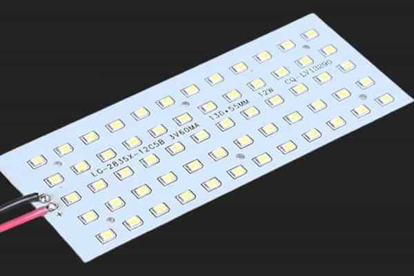
LED PCB boards are widely used in the lighting industry, such as plant growth lights.
Related Posts
- What is a Multilayer PCB and What are the Advantages?
- Angle Control in Multilayer PCB
- Custom Circuit Board Printing
- Top PCB Board Manufacturer And Supplier In China
- The Best And Fastest PCB Manufacturer In China
- Custom PCB Manufacturer In China
- Why Choose Chinese PCB Manufacturer
- How to Store PCB and PCBA?
- What Is FR-4 Material In PCB Fabrication?
- What Are the Multilayer PCB Applications?