


Introduction
In today’s fast-evolving electronics industry, the choice of PCB surface finish plays a critical role in ensuring reliability and performance. PCB Immersion Gold (ENIG) has emerged as a leading solution, offering superior solderability and oxidation resistance for modern printed circuit boards. Whether you’re designing complex devices with BGAs or seeking lead-free compliance, ENIG delivers unmatched durability. This article dives into what makes ENIG a preferred surface finish, its benefits and challenges, and how it’s manufactured, providing insights for engineers and manufacturers alike.
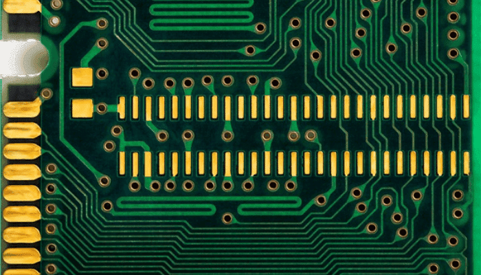
Table of Contents
What Is PCB Immersion Gold (ENIG) Surface Finish?
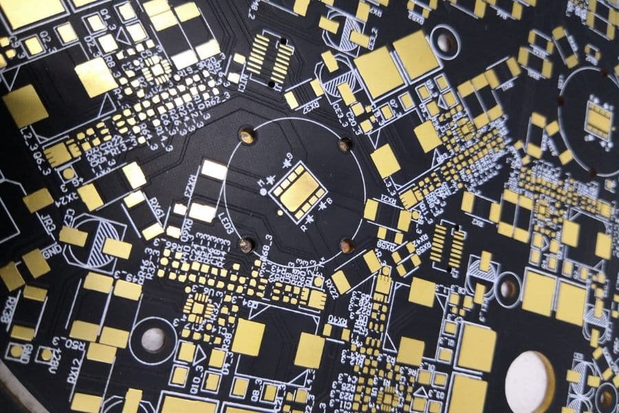
Electroless Nickel Immersion Gold (ENIG), also known as soft gold or chemical Ni/Au, is a widely used surface finish in PCB manufacturing. This process involves depositing a nickel-phosphorus alloy on a catalyzed palladium surface, followed by a thin gold coating. ENIG enhances PCB solderability, prevents oxidation of copper contacts and plated through-holes (PTH), and ensures reliable performance in various electronic applications.
Unlike traditional gold plating, ENIG offers improved durability and compatibility with lead-free soldering requirements. It’s ideal for complex components like Ball Grid Arrays (BGAs) and flip chips, making it a go-to choice in the PCB industry.

Key Benefits of ENIG Surface Finish for PCBs
ENIG has become a leading PCB surface finish due to its numerous advantages. Below are the key benefits:
Easy-to-Process Structure
Compared to Hot Air Solder Leveling (HASL) or Nickel Palladium, ENIG is simpler to process, particularly for solderability. Its straightforward structure streamlines PCB production, saving time and effort.
Flat Surface for Complex Components
ENIG provides a flat surface, essential for lead-free soldering and mounting intricate components like BGAs and flip chips. This ensures precision and reliability in advanced electronic designs.
Superior Oxidation Resistance
The electroless nickel layer, coated with immersion gold, significantly reduces oxidation risks. This protects the nickel from corrosion, ensuring long-term PCB reliability.
Optimal Electrical Performance
ENIG enhances the electrical performance of PCBs by ensuring stable connections. Precise design and high-quality surface finishing contribute to consistent signal integrity.
High Temperature Resistance
ENIG withstands high temperatures, preventing material expansion or damage to transmission lines. This minimizes issues like frequency shifts, distortion, or circuit board failure, extending PCB lifespan.
Lead-Free Compliance
ENIG is 100% lead-free, aligning with RoHS requirements and reducing health risks associated with lead exposure, such as anemia or kidney damage.
Additional Benefits
- Ideal for Plated Through-Holes (PTH): ENIG supports reliable PTH connections.
- No Electroplating Required: Simplifies the manufacturing process.
- Easy Welding: Compared to HASL or ENEPIG, ENIG is easier to weld.
Applications of ENIG Surface Finish in Modern Electronics
PCB Immersion Gold (ENIG) is widely used in applications requiring high reliability and performance. Its flat surface and excellent solderability make it ideal for:
- Consumer Electronics: Smartphones and tablets use ENIG for compact, high-density BGAs.
- Automotive Electronics: ENIG ensures durability in harsh environments, such as engine control units.
- Medical Devices: Lead-free ENIG supports biocompatible PCBs for implants and diagnostics.
- High-Frequency Applications: Despite potential signal loss, ENIG is used in 5G and RF circuits with careful design.
These applications highlight why ENIG is a go-to choice for modern PCB manufacturing. Learn more about choosing the right surface finish for your project here.

Disadvantages of ENIG Surface Finish
While ENIG offers significant advantages, it also has some drawbacks to consider:
Higher Cost
ENIG is more expensive than other surface finishes like HASL or OSP due to the high cost of gold, which may impact budget-conscious projects.
Black Pad Risk
Black pad occurs when phosphorus builds up between the gold and nickel layers, potentially causing fractured surfaces or faulty connections.
Limited Reworkability
ENIG-finished PCBs are less reworkable, with rigid structures that pose limitations during modifications.
Potential Signal Loss in RF Applications
The electroless nickel in ENIG can cause signal loss in high-frequency applications, impacting performance in RF circuits.
Complex Manufacturing Process
Designing and applying ENIG requires specialized knowledge and skills, making the process more intricate than other finishes.
How Is PCB Immersion Gold (ENIG) Surface Finish Manufactured?
The ENIG manufacturing process is complex but ensures a high-quality PCB surface finish. Here’s a step-by-step overview:
- Surface Preparation: Panels are cleaned, micro-etched, and activated to ensure a smooth base for coating.
- Nickel Deposition: The cassette is plunged into a nickel electroplating bath for approximately 22 minutes, depositing a 5-micron nickel layer.
- Gold Immersion: A thin gold layer (0.06 microns) is applied over the nickel through a displacement reaction.
- Quality Control: The panels are rinsed, dried, and inspected to ensure coating quality.
- Final Processing: Panels are transferred to the mechanical processing department for further assembly.
The final nickel thickness ranges from 100-200 microinches, while the gold layer is approximately 10-15 microinches. Automated systems monitor solution parameters, making adjustments to ensure consistency.
ENIG vs. Other PCB Surface Finishes: A Comparison
Surface Finish | Cost | Flatness | Oxidation Resistance | Best For |
|---|---|---|---|---|
ENIG | High | Excellent | Excellent | BGAs, lead-free PCBs |
HASL | Low | Poor | Moderate | Cost-sensitive projects |
OSP | Low | Good | Poor | Short-shelf-life PCBs |
ENEPIG | Very High | Excellent | Excellent | High-frequency, advanced PCBs |
ENIG balances flatness, solderability, and oxidation resistance, ideal for complex PCBs.
ENIG vs. Gold-Plated PCB: Key Differences
While both ENIG and gold-plated PCBs use gold, they differ significantly. ENIG uses a chemical deposition process, resulting in a thinner, more uniform gold layer, while gold plating involves electroplating a thicker layer. For a detailed comparison, read our article on ENIG vs. Gold-Plated PCBs.
FAQs About PCB Immersion Gold (ENIG) Surface Finish
What makes ENIG better than HASL for PCBs?
ENIG offers a flatter surface, better oxidation resistance, and lead-free compliance, making it ideal for complex and high-reliability applications compared to HASL.
How does ENIG improve PCB solderability?
The thin gold layer ensures excellent solderability by protecting copper contacts and PTH from oxidation, enabling strong solder joints.
Is ENIG surface finish suitable for high-frequency applications?
While ENIG is versatile, its electroless nickel layer may cause signal loss in RF applications, so alternative finishes like ENEPIG may be considered.
Final Words
PCB Immersion Gold (ENIG) Surface Finish stands out for its excellent solderability, oxidation resistance, and lead-free properties, making it a top choice for modern PCB manufacturing. Despite challenges like higher costs and black pad risks, its benefits make it ideal for high-performance PCBs. Ready to explore ENIG for your next PCB project? Contact JHYPCB for expert advice or learn more about PCB surface finishes on our blog here.


