Quick answer: OSP (Organic Solderability Preservative) is a water-based organic film chemically bonded to bare copper — not a metal coating. It gives you the flattest pads of any PCB surface finish at the lowest cost, which makes it the default choice for high-volume consumer SMT boards. Its limits are real: 3–6 months of shelf life, one to two reflow cycles, no wire bonding, and a process that demands nitrogen reflow and strict humidity control to perform reliably.
Table of Contents
Introduction to PCB OSP Surface Finish
Surface finishing is one of the last steps in PCB fabrication, and one of the most consequential. Applied after solder mask, the finish protects exposed copper from oxidation and gives components a surface they can actually wet and bond to. The industry’s main options — ENIG, immersion tin, immersion silver, HASL and OSP — differ sharply in cost, flatness and process tolerance.
OSP stands out on two fronts: it is the cheapest metallic-free option, and its pads are perfectly flat. That combination explains why it dominates high-volume consumer electronics, where boards are assembled within weeks of fabrication and every cent of unit cost matters. It also explains why OSP fails badly in the wrong application — long storage, multiple reflow cycles, wire bonding, or uncontrolled shop-floor humidity.
This guide covers what OSP is, how it is applied, where it wins and where it breaks down, how to store OSP boards, and how it compares with ENIG, immersion silver and lead-free HASL. For a full comparison of all ten PCB surface finishes, see our PCB surface finish selection guide.
What Is a PCB Surface Finish?
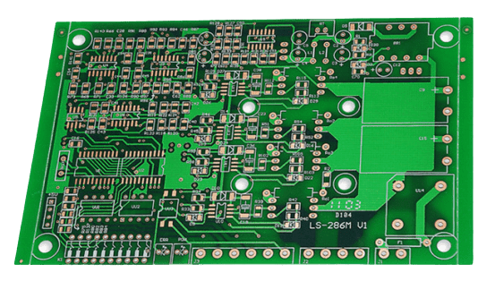
A PCB surface finish is a protective layer applied over exposed copper — pads, vias, test points and connector fingers — after solder mask and before assembly. It does three jobs:
- Preserves solderability. Bare copper oxidizes within hours of exposure, and oxidized copper will not wet reliably. The finish blocks that oxidation until the board reaches the reflow oven.
- Protects copper through fabrication and shipping. Boards pass through multiple cleaning, handling and packaging steps before they are populated.
- Provides a bondable interface. The right finish determines whether the pad can take solder only, or also wire bonds, press-fit pins, or repeated connector mating.
Finishes fall into two families. Metallic finishes — ENIG, ENEPIG, immersion tin, immersion silver, hard gold and HASL — deposit a metal layer that physically shields the copper. Organic finishes — OSP and anti-tarnish coatings — form a chemical film only a few molecules thick. Organic films are cheaper and flatter, but they offer no physical barrier, which is precisely why their process requirements are stricter.
The choice affects far more than cost. It determines which assembly processes your board can survive, how long you can warehouse it, whether it can pass RoHS and WEEE requirements for your target market, and — in the case of fine-pitch and BGA work — whether the solder joint forms at all.
Factors Influencing Surface Finish Selection
Six factors drive the decision in practice. They rarely point in the same direction, which is why surface finish selection is a trade-off exercise rather than a lookup.
- Application and reliability class. High-frequency and high-reliability designs generally need a metallic finish; consumer products with short assembly cycles can usually use OSP.
- Assembly process. How many reflow passes, whether there is wave or selective soldering, and whether the second side is populated after the first.
- Component types. BGA, QFN and anything at 0.5 mm pitch or below requires flat pads, which rules out HASL immediately.
- Storage and logistics. Time between fabrication and assembly, warehouse humidity, and whether boards ship overseas before use.
- Environmental compliance. RoHS and WEEE requirements for the destination market eliminate leaded HASL in most export products.
- Cost and volume. The finish is priced per panel; at high volume the difference between finishes becomes a meaningful line item, at prototype volume it is noise.
In practice, most projects can be narrowed to two candidates using just the component type and storage window, and then decided on cost. If you are weighing OSP against alternatives, our selection guide walks through all ten finishes in one matrix.
What Is OSP Surface Finish?
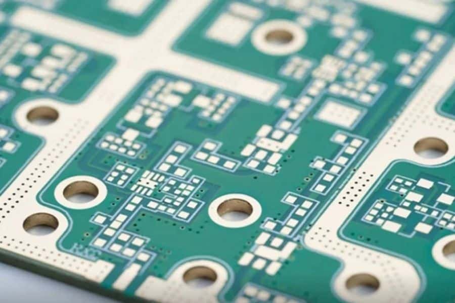
OSP — Organic Solderability Preservative — is a water-based organic compound applied to bare copper to prevent oxidation and preserve solderability. It is not a metal. The chemistry bonds selectively to copper, forming a transparent film typically 0.2–0.5 µm thick, which is thin enough to disappear completely into the solder joint during reflow.
Because the film is applied by simple immersion or spray in a horizontal line, OSP is fast, cheap and compatible with lead-free processes. It contains no metals, no cyanide and no formaldehyde, which makes it one of the most environmentally benign finishes available — and the reason it spread rapidly across the industry after the RoHS directive pushed leaded HASL out of consumer products.
Two properties define how OSP behaves in the factory:
- It is sacrificial. The film protects copper until the moment of soldering, then burns away. It does not reinforce the joint or add a barrier layer.
- It is invisible. There is no metallic sheen to inspect, so visual AOI cannot confirm that the coating is present and intact. Quality depends on process control, not on visual verification.
That second point is worth emphasising, because it is the root of most OSP assembly problems. A board that looks perfect can have a compromised coating, and the failure only appears as poor wetting or non-wetting at reflow.
OSP Surface Finish Manufacturing Process
The OSP line is short — four steps on a horizontal conveyor — but each one is a place where quality can be lost.
1. Cleaning. Organic contaminants, oils, fingerprints and copper oxide are removed so the chemistry can bond uniformly. Residual contamination here produces patchy coating that fails locally, and local failures are the hardest defects to trace.
2. Micro-etching (topography enhancement). A controlled etch roughens the copper surface at microscopic scale, increasing the area available for bonding and improving adhesion. The etch depth must stay in a narrow window: too little and the coating does not anchor; too much and you thin the copper and expose laminate.
3. De-ionized water rinsing. Residual ions from cleaning and etching are flushed away. Ionic contamination in the OSP bath shortens its life and produces uneven film formation — this is where water quality and bath maintenance show up.
4. Film formation. The board passes through the OSP bath, then through a de-ionized rinse held at pH 4.0–7.0 to prevent tarnish. Coating thickness, bath concentration, pH, temperature and dwell time all sit in a tight process window.
Bath life is finite and must be monitored by titration against copper concentration. This is the single biggest quality variable in OSP, and the reason two fabricators quoting “OSP” can deliver very different results. Ask for bath analysis records if the application is demanding.

Advantages of OSP Surface Finish
Perfectly flat pads. The film is a few tenths of a micron thick and follows the copper exactly. In practice OSP pads are as flat as any finish on the market, which makes it suitable for BGA and fine-pitch components down to 0.4 mm and below. No other low-cost finish comes close on coplanarity.
The lowest cost of any PCB finish. OSP is typically 0.9–1.0× the cost of lead-free HASL and a fraction of ENIG’s 1.3–2.0×. No gold, nickel or silver in the bath means both material cost and process cost drop, and the short line keeps cycle time down.
Environmentally clean. Water-based chemistry, no heavy metals, fully RoHS and WEEE compliant. There is no cyanide waste stream and no gold-bearing effluent to treat.
Fast and simple process. The horizontal line runs quickly and integrates easily with lead-free assembly. Turnaround from copper finish to shipping is measured in hours, not shifts.
Reworkable. If the coating is damaged, the board can be re-cleaned and re-coated. This is a real advantage in high-mix shops where boards get handled repeatedly.
Excellent solderability on the first pass. Fresh OSP wets very well — as good as any metallic finish in the first reflow, which is why it dominates single-pass consumer assembly.

Disadvantages of OSP Surface Finish
Short shelf life. This is the defining limitation. OSP is typically good for 3–6 months in moisture-barrier packaging, and far less once the bag is opened — often 8–24 hours depending on shop humidity, because the coating degrades on exposure to moisture and airborne contaminants. Plan assembly around the coating’s life, not against it.
Only one to two reflow cycles. Each thermal excursion consumes part of the film. Double-sided boards should put the OSP side through the first reflow, with the second pass as the practical maximum. Beyond that, pads begin to non-wet, especially on large thermal-mass areas.
No wire bonding. OSP cannot support gold or aluminium wire bonding. If the design includes bare die or wire-bonded interconnects, OSP is eliminated before cost is even discussed.
Nitrogen reflow strongly recommended. Without a metallic barrier, the copper immediately around the pads oxidizes at reflow temperature. Nitrogen inerting is not optional for fine-pitch and BGA work, and it adds cost that is easy to overlook when comparing quotes.
Invisible and easily damaged. The coating cannot be verified visually. Handling without gloves, scratches from handling or packaging, and solder-paste misprints all compromise it. Cleaning a misprint often removes the coating along with the paste, and pre-assembly baking can degrade it beyond recovery.
Thermal limits. Extended bake cycles — the standard remedy for moisture-sensitive boards — can damage OSP. If your assembly flow includes a 125 °C bake, verify the OSP chemistry can take it, or expect to re-coat.
How to Store OSP PCBs
Storage is where OSP boards are most often lost. The coating is a chemical barrier, not a physical one, and it degrades continuously from the moment of fabrication.
Packaging. Vacuum or moisture-barrier bags with desiccant and a humidity indicator card. Insert release paper between boards to prevent friction damage to the coating. Keep the bag sealed until the line is ready.
Environment. 15–30 °C and 30–70% relative humidity, away from direct sunlight and away from sulfur-bearing or acidic atmospheres — warehouse air near plating or etching operations is a common culprit.
Time limits. Consume within the stated shelf life (3–6 months from fabrication date), and treat the bag-opening clock as the real deadline. Record the opening date on the bag; a board that is 4 months old and has been open for three days is at risk regardless of the printed date.
Handling. Gloves at all times. No stacking without interleave. No wiping with solvents.
Two practical rules that prevent most incidents: order OSP boards against your assembly date, not your inventory plan, and if you cannot guarantee the assembly window, choose a finish whose shelf life you can live with.
Key Considerations for Assembling OSP PCBs
Place the OSP side first. In double-sided assembly, run the OSP side through the first reflow so the coating faces the fewest thermal cycles. Plan panel rotation accordingly.
Use nitrogen. For fine pitch, BGA and any board with tight wetting windows, nitrogen reflow is the difference between a stable process and a marginal one.
Control the paste and the printer. Paste volume and misprint handling matter more on OSP than on metallic finishes, because a misprint cannot be cleaned without risking the coating. Fix the printer rather than the board.
Check the bake policy. If the board needs a pre-assembly bake for moisture sensitivity, confirm with the fabricator whether the OSP chemistry survives it, and at what temperature and duration.
Watch the thermal profile. Ramp rates and peak temperature should sit inside both the solder paste and the OSP chemistry windows. Very long reflow profiles consume the film at the edges of large pads first.
Plan for inspection reality. Since the coating cannot be seen, rely on first-article wetting checks and process data rather than AOI alone. A simple solderability test on a coupon from each lot catches coating problems before they reach the line.
Design for it. Keep pad geometry consistent, avoid unnecessarily large exposed copper areas, and give test points the same treatment as component pads.

Why Is OSP So Widely Used?
Before 2005, leaded HASL was the default finish for most of the industry: cheap, forgiving and battle-tested. RoHS and WEEE changed that calculation by pushing lead out of consumer electronics, and manufacturers needed a lead-free finish that did not raise cost. ENIG was technically superior but too expensive for high-volume consumer boards; immersion silver cost more and needed sulfur-free handling.
OSP fitted the gap exactly. It was already qualified, it was the cheapest lead-free option, it needed no new metallurgy, and it delivered the flatness that the shift to SMT and fine-pitch components demanded. The result is the pattern you see today: OSP dominates televisions, set-top boxes, appliances, power supplies and other high-volume consumer boards assembled on short cycles, while ENIG takes the high-reliability, fine-pitch and bonding applications.
That split is not arbitrary — it tracks the two variables that matter most: assembly window and pad flatness requirement.
OSP vs. ENIG vs. Immersion Silver vs. Lead-Free HASL
The table below compares OSP against the three finishes it is most often weighed against. Costs are relative, with lead-free HASL as the 1.0× reference.
| Feature | OSP | ENIG | Immersion Silver | Lead-Free HASL |
|---|---|---|---|---|
| Relative cost | 0.9–1.0× | 1.3–2.0× | 1.2–1.4× | 1.0× |
| Pad flatness | Excellent | Excellent | Excellent | Poor |
| Shelf life | 3–6 months | 12+ months | 6–12 months | 12+ months |
| Reflow cycles | 1–2 | 3+ | 2–3 | 3+ |
| Wire bonding | No | Yes (gold) | Limited | No |
| BGA / fine pitch | Excellent | Excellent | Excellent | Not suitable |
| Solderability (first pass) | Excellent | Excellent | Excellent | Good |
| Environmental profile | Water-based, RoHS/WEEE | Nickel effluent to treat | Silver bath to maintain | Lead-free alloy |
| Main risk | Oxidation after bag opening | Black pad, cost | Tarnish from sulfur | Uneven pads, thermal stress |
How to read the trade-offs:
- OSP vs ENIG is essentially a cost-versus-window decision. OSP wins on unit cost and equals ENIG on flatness; ENIG wins on shelf life, reflow cycles and bonding, and carries a black-pad risk that depends on process control. For boards with a fixed assembly date inside six months, OSP is very hard to beat on value.
- OSP vs immersion silver is closer than it looks. Both are flat and mid-to-low cost; silver tolerates more reflow cycles and bonds aluminium wire, but it tarnishes in sulfur-bearing air and costs more. OSP is the simpler, cheaper and more forgiving choice for consumer work.
- OSP vs lead-free HASL comes down to flatness. If there is no BGA or fine-pitch content, HASL’s lower process sensitivity and longer shelf life make it the pragmatic choice. The moment 0.5 mm pitch enters the design, HASL is out.
Each of these finishes has a dedicated guide: the lead-free HASL alternative in our Hot Air Solder Leveling (HASL) guide, the gold option in What Is PCB Immersion Gold (ENIG) Surface Finish?, and the silver option in our immersion silver PCB guide.
Conclusion
OSP is the most cost-efficient surface finish available, and on the right boards it is also the best-performing one: perfectly flat pads, excellent first-pass solderability, a clean environmental profile and a process fast enough to keep high-volume lines moving.
It is not a universal finish. The 3–6 month shelf life, the one-to-two reflow ceiling, the need for nitrogen and the absence of wire-bonding capability all place hard limits on where OSP belongs. Choose it when your boards are assembled on a short cycle, your components are SMT and flatness matters, and you can control storage and handling. Choose something else when any of those conditions cannot be guaranteed.
If you are unsure which side of that line your design falls on, send us the Gerber files — our engineers will review the stack-up, component mix and assembly flow, and recommend a finish with the DFM report.
FAQs About PCB OSP Surface Finish
Yes. OSP typically costs 0.9–1.0× lead-free HASL, while ENIG runs 1.3–2.0×. On high-volume consumer boards that meet OSP's process requirements, the difference is a significant line item in unit cost.
One to two. The film is consumed with each thermal exposure, so in double-sided assembly the OSP side should go through the first reflow, with a second pass as the practical maximum. Beyond that, pad non-wetting becomes likely.
Yes — for single-reflow, high-volume BGA assembly. OSP pads are as flat as ENIG pads, so coplanarity is not a problem. But if the boards will sit in storage for months, see multiple reflows, or need wire bonding, ENIG is the safer choice.
Typically 8–24 hours, depending on shop humidity and handling. The 3–6 month figure assumes a sealed moisture-barrier bag. Once opened, treat assembly as urgent and record the opening date.
Without a metallic barrier, the copper around OSP pads oxidizes quickly at reflow temperature. Nitrogen inerting suppresses that oxidation and is strongly recommended for fine-pitch and BGA work, where the wetting window is narrow.