Step Stencil Manufacturing
Precision-engineered stencils with multi-level thickness for advanced PCB assembly needs.
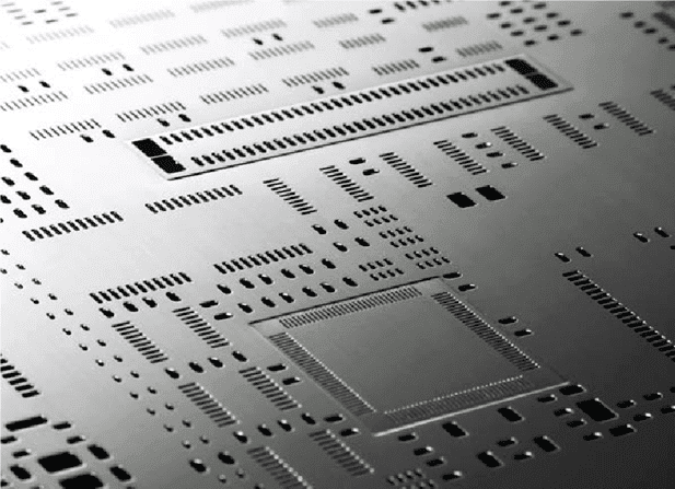
What is a Step Stencil?
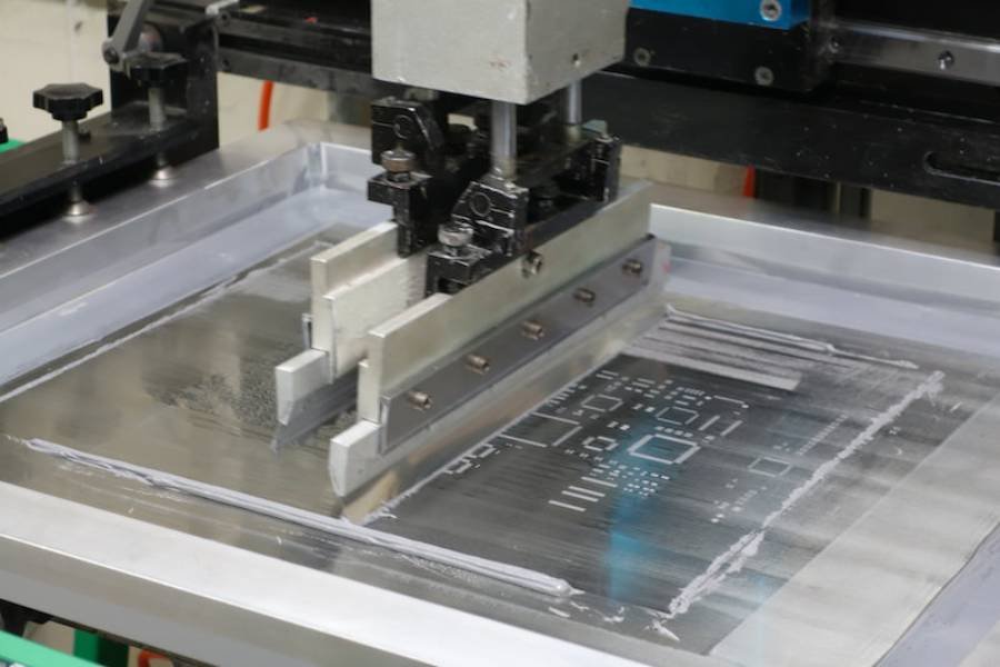
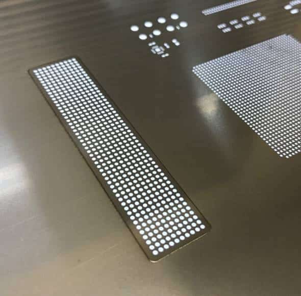
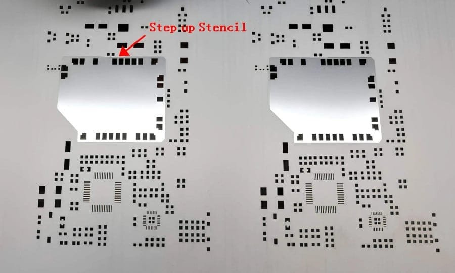
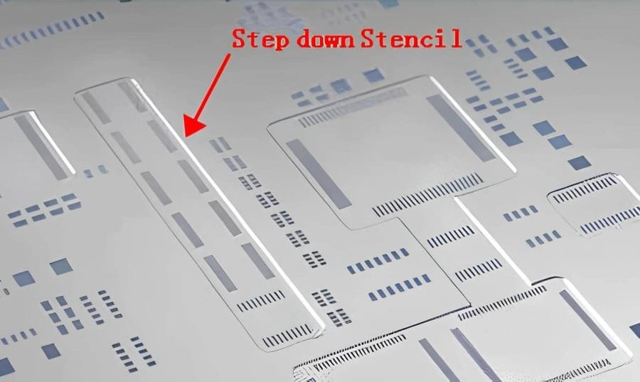
A Step Stencil, also known as a multi-level stencil, is an advanced tool used in Surface Mount Technology (SMT) assembly to apply precise amounts of solder paste to printed circuit boards (PCBs). Unlike standard stencils with uniform thickness, Step Stencils feature varying thickness levels—thicker areas for large components like Ball Grid Arrays (BGAs) and thinner areas for fine-pitch components like 0402 chips or Quad Flat Packages (QFPs). This design ensures optimal solder paste deposition for diverse component sizes on a single PCB, improving soldering quality and assembly efficiency.
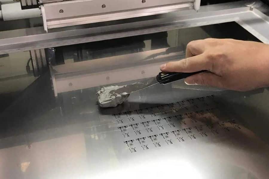
Step Stencils are critical for modern PCB designs, which often integrate a mix of miniature and large SMT components. By controlling solder paste volume with precision, they prevent common issues such as solder bridging, insufficient soldering, or paste smearing. At JHYPCB, our Step Stencils are crafted using high-precision laser cutting and advanced fabrication techniques like photo-chemical etching or laser welding, ensuring compatibility with complex PCB layouts and high-yield production.
Benefits of Step Stencils
- Precise Solder Paste Volume Control: Multi-level thickness design optimizes solder paste deposition for diverse components, such as BGAs and 0201 chips, reducing defects like solder bridging or insufficient joints.
- Simplified Assembly Process: A single Step Stencil eliminates the need for multiple stencils, streamlining SMT printing and minimizing setup time.
- Improved Paste Release Efficiency: Varying thickness levels enhance solder paste transfer, reducing smearing and ensuring consistent prints across complex PCB layouts.
- Versatility for Mixed Components: Supports PCBs with both large and fine-pitch components, enabling high-yield assembly for modern, compact electronics.
- Cost Efficiency: Optimizes solder paste usage and reduces rework by minimizing defects, lowering overall production costs.
Applications of Step Stencils
Step Stencils are essential for high-precision PCB assembly across various industries, enabling reliable solder paste deposition for complex, mixed-component designs.
Consumer Electronics
Supports compact devices like smartphones, wearables, and IoT gadgets, where miniature components like 0201 chips and large connectors coexist on dense PCBs.
Automotive Electronics
Ensures robust soldering for ECUs, sensors, and infotainment systems, accommodating diverse component sizes in harsh environments.
Medical Devices
Facilitates high-reliability assembly for diagnostic equipment, implants, and wearables, where precision and miniaturization are critical.
Telecommunications
Enables efficient production of 5G infrastructure, routers, and antennas, handling fine-pitch components and high-density layouts.
Aerospace and Defense
Supports mission-critical electronics like avionics and satellite systems, ensuring consistent soldering for complex, high-performance PCBs.
Our Step Stencil Manufacturing Process
Our advanced manufacturing process ensures precision and reliability for every Step Stencil, tailored to meet complex PCB assembly needs:
- Design Analysis: We review your PCB layout to determine optimal stencil thickness, aperture sizes, and step configurations for precise solder paste application.
- Fabrication Selection: We select the best technique—photo-chemical etching, micro-machining, or laser welding—based on your design complexity and performance requirements.
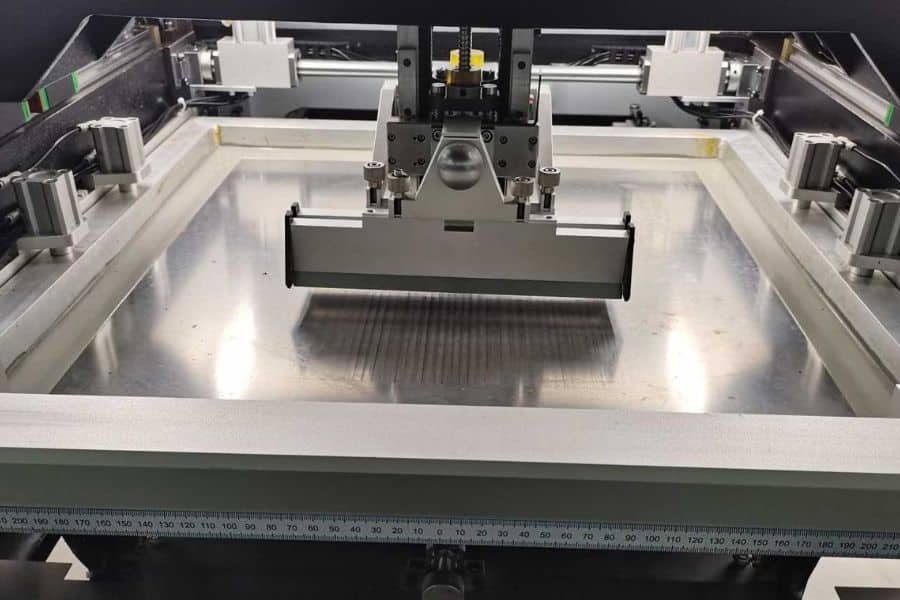
- Precision Laser Cutting: High-accuracy laser cutting creates apertures and multi-level steps, ensuring compatibility with fine-pitch and large components.
- Surface Enhancement: Optional electropolishing or nano-coating is applied to improve paste release and extend stencil durability.
- Quality Assurance: Rigorous inspections verify dimensional accuracy, step alignment, and aperture quality to guarantee consistent performance.
- Rapid Delivery: Efficient production and global shipping ensure your Step Stencil arrives on time to meet project deadlines.
Why Choose JHYPCB for Step Stencil Manufacturing?
JHYPCB delivers unmatched expertise and reliability in Step Stencil production, ensuring precision and efficiency for your SMT assembly needs: