Single Layer PCB Manufacturing | Affordable Single Sided PCBs
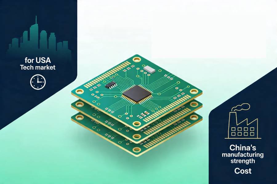
Partner with JHYPCB, a leading single layer PCB manufacturer in China, for cost-effective single sided PCB production, rapid prototyping, and free DFM checks. Ensure flawless quality for your LED lighting, power supplies, and more.
Leading Single Layer PCB Manufacturer - JHYPCB
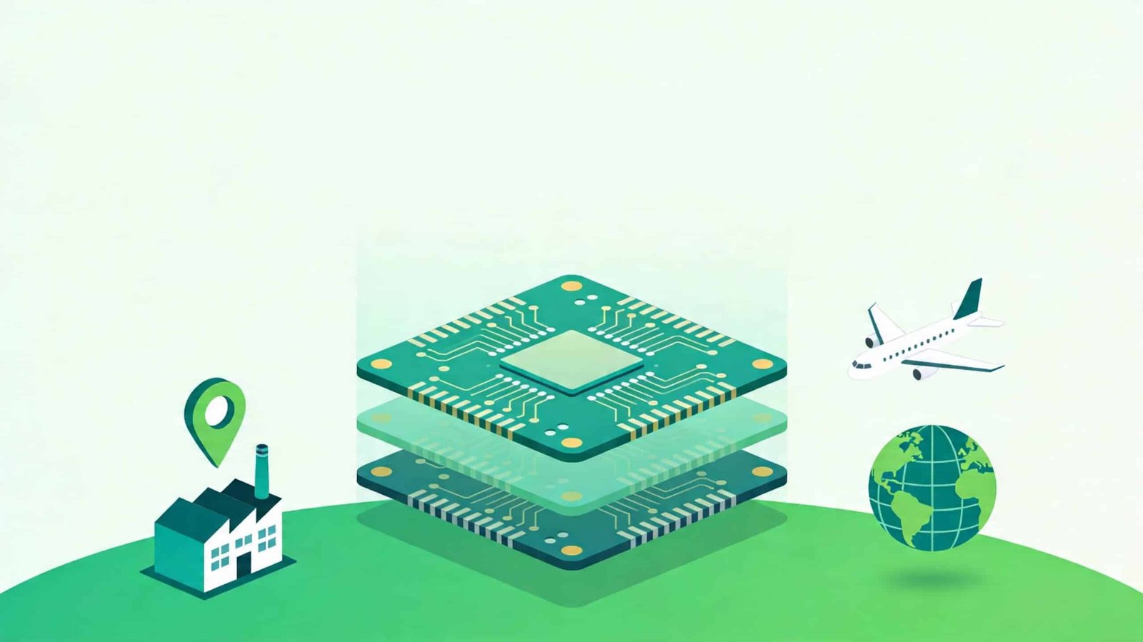
JHYPCB specializes in single layer PCB manufacturing, delivering reliable, cost-effective solutions for applications like LED lighting, calculators, and vending machines. Our ISO-certified process, fast prototyping, and free DFM checks guarantee top-quality single sided PCBs tailored to your needs.

Single-Layer PCB Definition
What is a Single Layer PCB?
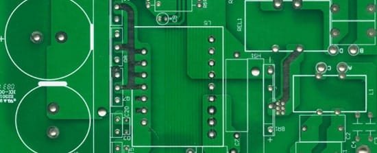
A single layer PCB, also known as a single sided PCB, features one conductive copper layer on a base material like FR-4 or aluminum. Protected by a solder mask and labeled with silkscreen, these PCBs are ideal for simple circuits in consumer electronics and industrial equipment. JHYPCB ensures high reliability with free DFM checks.
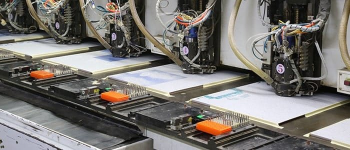
Single Layer PCB Manufacturing
Types of Single Layer PCBs
Made from durable FR-4, ideal for calculators and power supplies. JHYPCB offers fast prototyping and free DFM checks.
Pliable materials for wearable devices. JHYPCB ensures precision and affordability.
Combines rigid and flexible materials for cameras. JHYPCB delivers high-quality production.
Uses Rogers for RF equipment. JHYPCB ensures superior signal integrity.
Excels in heat dissipation for LED lighting. JHYPCB offers cost-effective solutions.
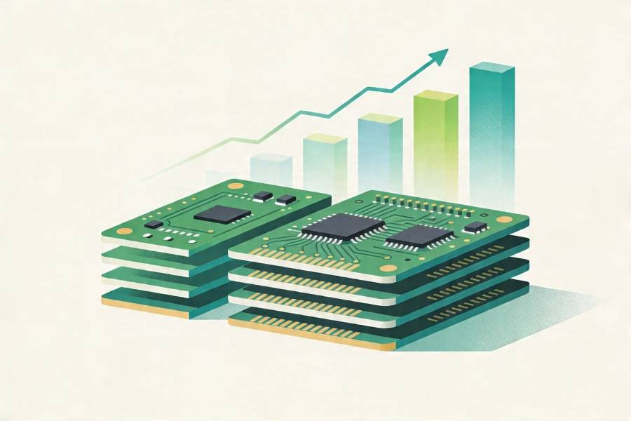
Benefits of Single Layer PCBs
Single Layer PCB Manufacturing Process
JHYPCB’s streamlined process ensures precision:
Step 1
Order & DFM Check
Order & DFM Check
Review Gerber files for flawless design.
Step 2
Material Preparation
Material Preparation
Use FR-4 or aluminum based on specifications.
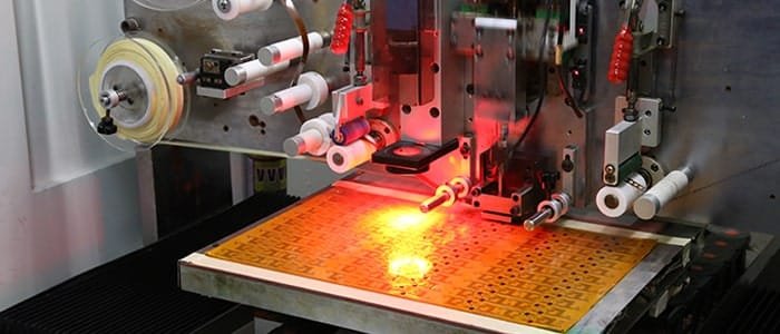
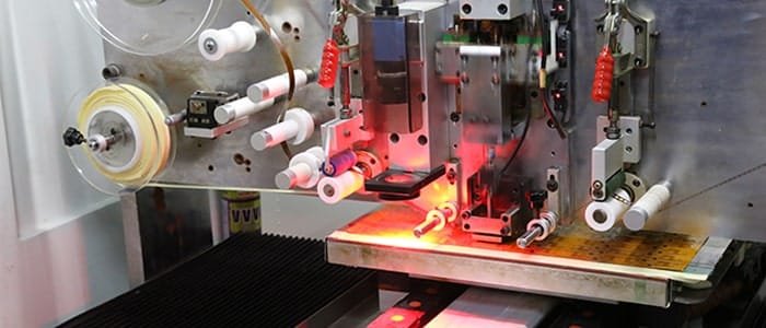
Step 3
Circuit Printing & Etching
Circuit Printing & Etching
Form precise copper traces.
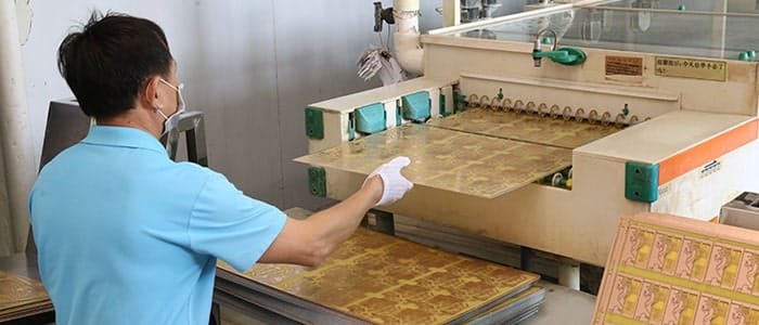
Step 4
Drilling & Plating
Drilling & Plating
Add holes for components.
Step 5
Solder Mask & Silkscreen
Solder Mask & Silkscreen
Protect circuits and add labeling.
Step 6
Testing
Testing
AOI and flying probe tests ensure reliability.
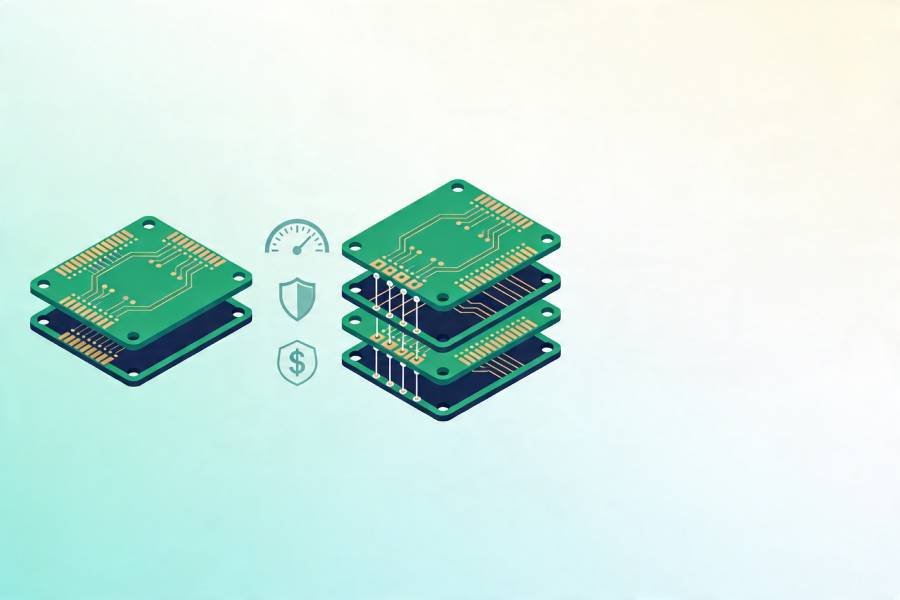
Single-Sided vs. Double-Sided vs. Multilayer PCBs
| Feature | Single-Sided PCB | Double-Sided PCB | Multilayer PCB |
|---|---|---|---|
| Conductive Layers | 1 | 2 | 3+ |
| Applications | Calculators, LED Lighting | Smartphones, Industrial Controls | Aerospace, Medical Devices |
| Cost | Low | Moderate | High |
| Complexity | Simple | Moderate | High |
Single-sided PCB FAQs
A single layer PCB has one conductive copper layer, ideal for simple circuits like LED lighting and sensors. JHYPCB delivers reliable single sided PCBs with fast production.
Single layer PCBs power devices like calculators, power supplies, and vending machines. JHYPCB ensures high-quality production for these applications.
Use standard FR-4 material and order in bulk. JHYPCB offers competitive pricing and rapid production for cost-effective single sided PCBs.
Typically 1.6mm, but JHYPCB customizes thickness for applications like industrial equipment or compact sensors.
Choose JHYPCB for Single Layer PCBs
Trust JHYPCB for high-quality single sided PCB manufacturing. Enjoy rapid production, free DFM checks, and competitive pricing for your LED lighting, power supplies, and more.