Table of Contents
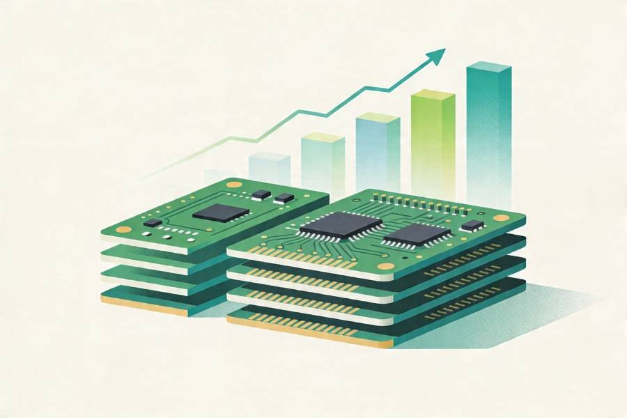
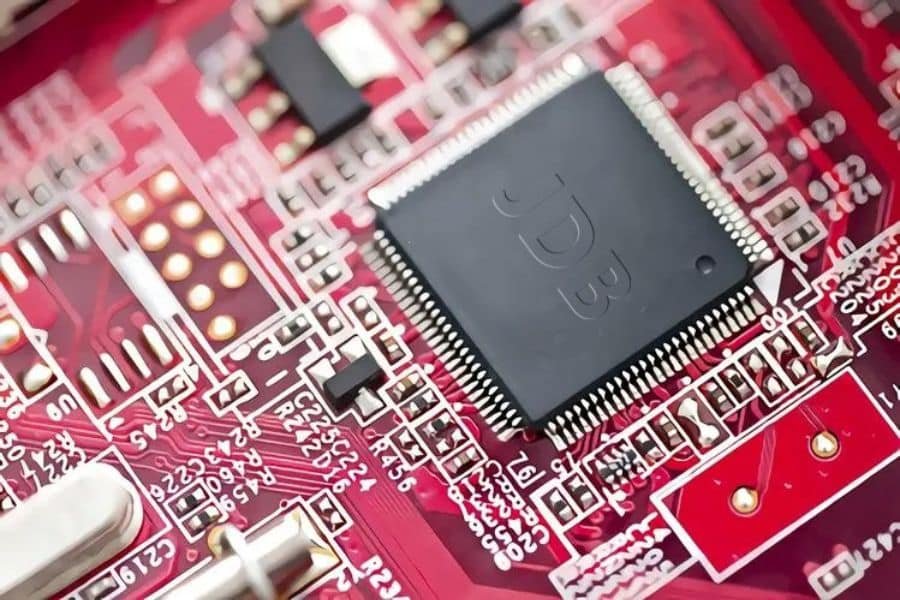
Printed Circuit Boards are the foundation of every modern electronic device — and among all PCB types, multilayer PCBs stand apart. A multilayer PCB is a circuit board with three or more conductive copper layers laminated together with insulating dielectric materials into a single compact stackup. Unlike single‑sided or double‑sided boards, multilayer PCBs can accommodate far greater circuit complexity, higher component density, and superior signal integrity in a fraction of the physical space — making them the go‑to choice for advanced electronics in telecommunications, automotive, medical, aerospace and consumer applications.
In this 2026 updated guide, we cover everything engineers, PCB designers and procurement teams need to know about multilayer PCBs: how they are structured, the key advantages and trade‑offs, typical applications and layer counts, the step‑by‑step manufacturing process, and practical strategies for cost optimization and design for manufacturability. Whether you are evaluating multilayer technology for a new project or looking to optimize an existing design, this guide will help you make informed decisions — from stackup selection to supplier qualification.
Drawing on years of multilayer PCB manufacturing experience — from 4‑layer prototype boards to complex 32‑layer HDI designs — the team at JHYPCB has compiled this guide to share practical insights that go beyond textbook theory, including real‑world tips on layer count decisions, material selection and DFM‑driven cost savings.
What is multilayer PCB?
A multilayer PCB is a sophisticated circuit board that consists of three or more conductive copper layers separated by insulating materials, known as dielectrics. Unlike single-sided PCBs, which have components and circuits on one side, or double-sided PCBs, which feature circuits on both sides connected via vias, multilayer PCBs stack multiple layers to accommodate complex and high-density circuitry. This design allows for greater functionality in a compact form, making them essential for advanced electronics like smartphones, medical devices, and aerospace systems.
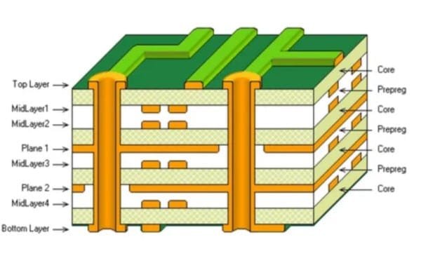
Structure of a Multilayer PCB
The construction of a multilayer PCB involves several key components, each serving a specific purpose to ensure reliable performance:
- Substrate/Dielectric: The insulating material (typically FR4, polyimide, or high-TG materials) that separates conductive layers, preventing unwanted electrical connections.
- Conductive Layers: Thin copper foils that form the circuit paths. These layers include inner layers (sandwiched within the board) and outer layers (on the board’s surface).
- Vias: Small, metal-coated holes that connect different layers electrically. Types include:
- Through-Hole Vias: Extend through the entire board, connecting all layers.
- Blind Vias: Connect an outer layer to one or more inner layers without passing through the entire board.
- Buried Vias: Connect inner layers without reaching the outer surfaces.
- Solder Mask: A protective layer (often green, but available in red, blue, or other colors) that covers the copper traces to prevent short circuits and oxidation.
- Silkscreen: A printed layer that adds labels, symbols, or component identifiers for assembly and maintenance.
- Surface Finish: A coating applied to exposed copper to enhance solderability and prevent oxidation. Common finishes include HASL (Hot Air Solder Leveling), ENIG (Electroless Nickel Immersion Gold), Immersion Silver, Immersion Tin, and OSP (Organic Solderability Preservative).
How Multilayer PCBs Differ from Single-Sided and Double-Sided PCBs
To understand the role of multilayer PCBs, it’s helpful to compare them with other PCB types:
- Single-Sided PCBs: Feature components and circuits on one side only. They are simple, cost-effective, and used in basic electronics like calculators or LED lighting. However, their single-layer design limits circuit complexity, as traces cannot cross without jumpers.
- Double-Sided PCBs: Have circuits on both sides, connected
through vias. They offer more design flexibility and are suitable for moderately complex devices like amplifiers or HVAC systems. However, their capacity is still limited compared to multilayer PCBs — for a detailed performance and cost breakdown, see our guide on multilayer PCB vs double-sided PCB. - Multilayer PCBs: With three or more layers, these boards support intricate designs and high component density. They are ideal for advanced applications requiring compact size, high-speed performance, and reliability, such as telecommunications equipment and medical imaging devices.
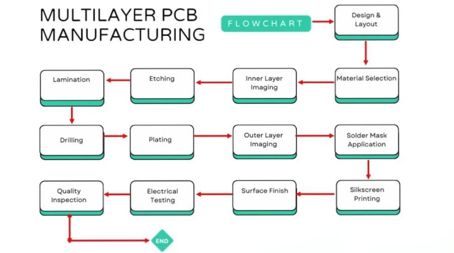
Manufacturing Overview
Creating a multilayer PCB is a complex process that requires precision and advanced technology. The process typically involves:
- Design and Layout: Engineers use CAD software to design the layer stackup and circuit patterns.
- Layer Preparation: Copper-clad cores and insulating prepreg materials are laminated together under heat and pressure.
- Drilling and Plating: Vias are drilled and plated with conductive material to connect layers.
- Etching and Finishing: Circuit patterns are etched, solder mask and silkscreen are applied, and a surface finish is added.
- Testing: Electrical and visual inspections, including X-ray analysis, ensure quality and functionality.
This intricate process enables multilayer PCBs to meet the demands of modern electronics, balancing performance, reliability, and compactness.
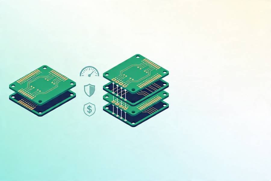
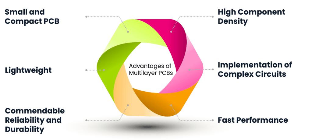
Advantages Of Multilayer PCBs vs Double-Sided & Single-Sided PCBs
Multilayer PCBs have become the go-to choice for advanced electronics due to their ability to meet the demands of complex, high-performance devices. Nowhere is this clearer than in the comparison of multilayer PCB vs double-sided PCB or single-sided PCB — multilayer boards deliver decisive gains in circuit density, signal integrity and form factor that simpler board types simply cannot match. By stacking multiple conductive layers, these boards enable compact designs, improved reliability and superior functionality.
1. Compact Size
One of the most significant advantages of multilayer PCBs is their compact size. By distributing circuitry across multiple layers, these boards can accommodate complex designs without requiring a large surface area. This makes them ideal for space-constrained devices like smartphones, wearables, and IoT modules. For example, a multilayer PCB can integrate intricate wiring and components into a fraction of the space needed for a single- or double-sided board, enabling sleek, portable products that meet modern design trends.
2. Lightweight Design
Multilayer PCBs eliminate the need for bulky wires, jumpers, or external connectors, resulting in a significantly lighter board. The use of surface-mount devices (SMDs) further reduces weight by allowing compact component placement. This lightweight design is critical for applications like drones, portable medical devices, and handheld gadgets, where minimizing weight enhances performance and user experience.
3. High Reliability and Durability
The internal connections between layers in a multilayer PCB are more robust than external connectors used in simpler boards. These connections, formed through vias and precise lamination, reduce the risk of failure due to vibration, thermal stress, or environmental factors. Additionally, the use of high-quality materials like FR4 or high-TG substrates ensures that multilayer PCBs can withstand extreme conditions, making them highly reliable for applications in aerospace, automotive, and industrial systems.
4. High Component Density
Multilayer PCBs support a higher density of components compared to single- or double-sided boards. By utilizing both sides of the board and multiple internal layers, designers can place more components in a smaller area. Surface-mount technology further enhances this capability by allowing compact, high-performance components like microchips and resistors to be densely packed. This advantage is crucial for devices like tablets and servers, where maximizing functionality in limited space is essential.
5. Support for Complex Circuits
The additional layers in a multilayer PCB provide greater routing flexibility, enabling the implementation of intricate and sophisticated circuit designs. This is particularly important for applications requiring high-speed data processing, such as 5G telecommunications equipment or advanced computing systems. Unlike single-sided PCBs, where traces cannot cross without jumpers, multilayer PCBs allow designers to create complex layouts with minimal interference, ensuring optimal signal integrity.
6. Enhanced Performance
Multilayer PCBs deliver superior performance due to their optimized design. The shorter interconnection paths between layers reduce signal transmission delays, improving speed and efficiency. Additionally, multilayer PCBs allow better control of differential and single-ended impedance, which is critical for high-frequency applications like RF communication devices. This results in reduced crosstalk, improved signal quality, and reliable performance in demanding environments.
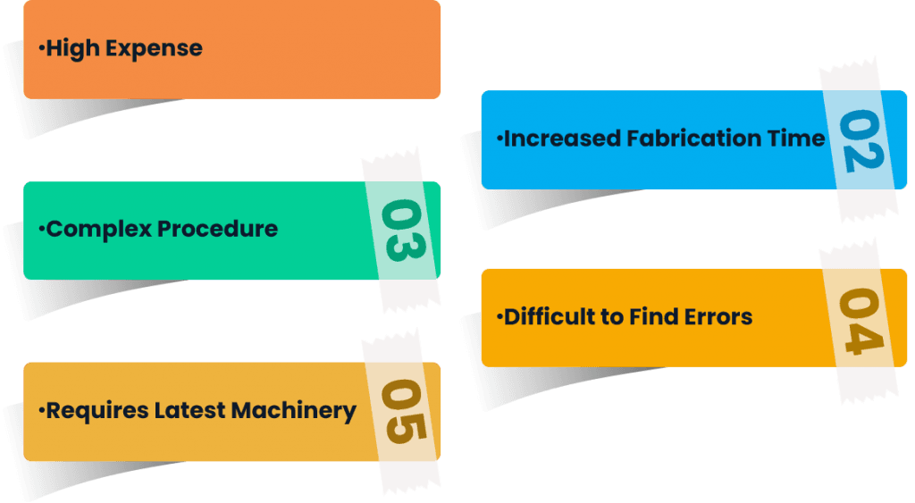
Disadvantages Of Multilayer PCBs vs Double-Sided & Single-Sided PCBs
While multilayer PCBs offer significant advantages for complex and high-performance electronics, they also come with certain challenges — particularly when compared against the simplicity and lower cost of a single-sided or multilayer PCB vs double-sided PCB scenario. These drawbacks, such as higher costs and intricate production processes, can impact project timelines, budgets and feasibility. Understanding these limitations is crucial for making informed decisions about whether a multilayer PCB is the right choice for your application.”
1. Higher Cost
Multilayer PCBs are more expensive to design and manufacture compared to single-sided or double-sided PCBs. The increased cost stems from the complexity of the design, which requires additional layers, precise alignment, and advanced materials like high-TG substrates or low-loss dielectrics. Furthermore, the need for specialized equipment and skilled engineers adds to the overall expense. While the compact size and performance benefits often justify the cost for high-end applications like smartphones or medical devices, budget-conscious projects may find multilayer PCBs less economical.
2. Complex Manufacturing Process
The production of multilayer PCBs involves intricate processes that demand high precision and expertise. Tasks such as layer alignment, via drilling (including blind and buried vias), and lamination require advanced machinery and experienced technicians. Any misalignment or defect in a single layer can compromise the entire board, leading to costly rework or scrapping. This complexity makes multilayer PCB manufacturing less accessible for smaller manufacturers without the necessary infrastructure, limiting production options.
3. Longer Fabrication Time
Due to the multiple layers and sophisticated processes involved, multilayer PCBs take longer to produce than single- or double-sided boards. Each layer requires careful design, etching, lamination, and testing, which extends the overall fabrication timeline. For instance, while a single-sided PCB prototype might be completed in a day, a multilayer PCB with 4–8 layers could take 3–5 days or more, depending on complexity. This extended lead time can be a challenge for projects with tight deadlines.
4. Difficult Repairs and Troubleshooting
Identifying and fixing issues in multilayer PCBs is significantly more challenging than in simpler boards. The hidden inner layers and dense component placement make it difficult to pinpoint faults without specialized equipment, such as X-ray inspection systems. Repairs, when possible, often require advanced skills and tools, increasing maintenance costs. In some cases, a defective multilayer PCB may need to be replaced entirely, which can be costly and time-consuming, particularly in critical applications like aerospace or medical systems.
Applications of Multilayer PCBs
Multilayer PCBs are the backbone of modern electronics, enabling compact, high-performance devices across a wide range of industries. Their ability to support complex circuits, high component density, and reliable performance makes them indispensable in applications where space, speed, and durability are critical. From smartphones to satellite systems, multilayer PCBs power cutting-edge technology in diverse sectors. Below, we explore the key applications of multilayer PCBs, highlighting their role in driving innovation and efficiency.
1. Consumer Electronics
Multilayer PCBs are ubiquitous in consumer electronics, where compact size and high functionality are paramount. Devices like smartphones, tablets, smartwatches, and laptops rely on multilayer PCBs (typically 4–12 layers) to integrate processors, memory, and sensors into small form factors. For example, a smartphone’s multilayer PCB enables seamless connectivity, high-speed processing, and power efficiency, supporting features like 5G, touchscreens, and cameras in a sleek design.
2. Telecommunications
The telecommunications industry heavily depends on multilayer PCBs for high-speed and reliable data transmission. Equipment such as 5G base stations, routers, modems, and satellite communication systems use multilayer PCBs to handle complex signal routing and high-frequency performance. These boards ensure low signal loss and controlled impedance, critical for maintaining connectivity in modern networks and supporting the growing demand for IoT and 5G technologies.
3. Automotive
Modern vehicles, especially electric vehicles (EVs) and those with advanced driver-assistance systems (ADAS), rely on multilayer PCBs for their sophisticated electronics. These boards power systems like infotainment, navigation, collision avoidance, and battery management. Their durability and ability to support high component density make multilayer PCBs ideal for the harsh environments of automotive applications, ensuring reliable performance under temperature fluctuations and vibrations.
4. Healthcare
In the healthcare sector, multilayer PCBs are critical for advanced medical devices that require precision and reliability. Equipment such as MRI machines, CT scanners, pacemakers, and wearable health monitors use multilayer PCBs to integrate complex circuits in compact, lightweight designs. These boards enable high-speed data processing and accurate signal transmission, ensuring patient safety and diagnostic accuracy in critical medical applications.
5. Aerospace and Defense
Multilayer PCBs are essential in aerospace and defense applications, where reliability and performance under extreme conditions are non-negotiable. Avionics systems, radar equipment, satellite navigation, and military communication devices rely on multilayer PCBs to handle high-frequency signals and dense circuitry. Their robust construction ensures functionality in high-vibration, high-temperature, and radiation-heavy environments, making them a staple in mission-critical systems.
6. Industrial IoT and Automation
The rise of Industrial IoT (IIoT) and automation has increased the demand for multilayer PCBs in smart factories and industrial systems. These boards power sensors, controllers, and communication modules used in robotics, automated machinery, and environmental monitoring systems. Their ability to support high-density interconnects and reliable performance ensures seamless data exchange and operational efficiency in Industry 4.0 applications.

Recent Trends in Multilayer PCB Development
As the demand for smaller, faster, and more efficient electronics continues to grow, multilayer PCBs are evolving to meet the needs of cutting-edge applications. Innovations in design, materials, and manufacturing processes are driving the development of multilayer PCBs, enabling them to support emerging technologies like 5G, IoT, and artificial intelligence. These advancements are shaping the future of the electronics industry, from consumer devices to industrial automation. Below, we explore the key trends in multilayer PCB development that are redefining performance and functionality.
1. High-Density Interconnects (HDI)
High-density interconnect (HDI) technology is a major trend in multilayer PCB development, enabling finer lines, smaller vias, and higher component density. HDI PCBs use micro vias, blind vias, and buried vias to achieve compact designs, making them ideal for smartphones, wearables, and medical implants. This trend supports the miniaturization of electronics while maintaining high performance, addressing the growing need for smaller yet more powerful devices.
2. Flexible and Rigid-Flex PCBs
Flexible and rigid-flex multilayer PCBs are gaining popularity in applications requiring adaptability and durability. Flexible PCBs, made from materials like polyimide, can bend and fold, making them suitable for wearables, foldable smartphones, and automotive sensors. Rigid-flex PCBs combine the benefits of rigid and flexible boards, offering structural stability and flexibility for complex designs in aerospace and medical devices.
3. Advanced Materials for High-Frequency Applications
The rise of 5G, IoT, and high-speed computing has driven the adoption of advanced materials in multilayer PCBs. Low-loss dielectrics, such as PTFE and high-TG FR4, are increasingly used to minimize signal loss and improve performance in high-frequency applications like 5G base stations and radar systems. These materials enhance signal integrity and thermal management, ensuring reliability in demanding environments.
4. Sustainability and Eco-Friendly Materials
Sustainability is becoming a priority in PCB manufacturing, with a focus on eco-friendly materials and processes. Manufacturers are exploring halogen-free substrates, recyclable dielectrics, and lead-free surface finishes to reduce environmental impact. Additionally, efforts to improve material efficiency and implement recycling programs are aligning multilayer PCB production with global sustainability goals, appealing to environmentally conscious industries.
5. 5G and IoT Integration
The rollout of 5G networks and the expansion of the Internet of Things (IoT) are driving demand for multilayer PCBs optimized for high-speed, low-power performance. These PCBs are designed with precise impedance control and compact layouts to support 5G antennas, IoT sensors, and edge computing devices. This trend is particularly relevant in telecommunications, smart cities, and industrial IoT, where connectivity and efficiency are critical.
6. AI and Automation in Design and Manufacturing
Artificial intelligence (AI) and automation are transforming multilayer PCB design and production. AI-driven design tools optimize layer stackups, signal routing, and thermal management, reducing design time and errors. Automated manufacturing processes, such as robotic assembly and advanced inspection systems, improve precision and efficiency, enabling faster production of complex multilayer PCBs for applications like autonomous vehicles and smart factories.

Multilayer PCB Manufacturing Process Step by Step
The manufacturing of multilayer PCBs is a complex and precise process that transforms a design concept into a functional circuit board capable of powering advanced electronics. Unlike single- or double-sided PCBs, multilayer PCBs require meticulous layer alignment, advanced materials, and sophisticated equipment to ensure reliability and performance. This process involves multiple stages, from initial design to final testing, each critical to producing high-quality boards for applications like telecommunications, medical devices, and automotive systems. Below, we outline the key steps in the multilayer PCB manufacturing process, providing insight into the technology and expertise involved.
1. Design and Layout
The process begins with designing the multilayer PCB using Computer-Aided Design (CAD) software. Engineers create a detailed layout, defining the circuit patterns, layer stackup, and via placements. The stackup specifies the arrangement of conductive copper layers and insulating dielectric materials (e.g., FR4 or polyimide). Design rules, such as trace width, spacing, and impedance control, are carefully planned to meet the application’s electrical and thermal requirements. This stage also involves generating Gerber files, which serve as blueprints for manufacturing.
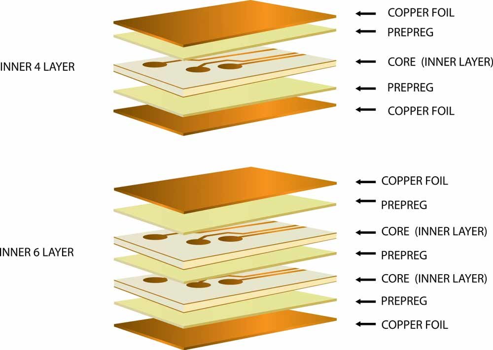
2. Core and Prepreg Preparation
Multilayer PCBs are constructed using core materials (thin copper-clad laminates) and prepreg (pre-impregnated resin sheets) as the insulating layers. The core layers, typically made of FR4 or high-TG materials, have copper foil on both sides, forming the inner circuit layers. Prepreg sheets, which harden during lamination, are placed between cores to bond the layers together. These materials are cut to size and prepared for patterning, ensuring precise alignment for the subsequent steps.
3. Inner Layer Patterning and Etching
The inner layers are patterned by applying a photoresist coating to the copper surfaces of the core materials. A photolithographic process transfers the circuit design onto the photoresist using UV light and a mask. The exposed copper is etched away, leaving the desired circuit patterns. This step requires high precision to ensure accurate trace widths and spacing, as errors in inner layers can affect the entire board’s functionality.
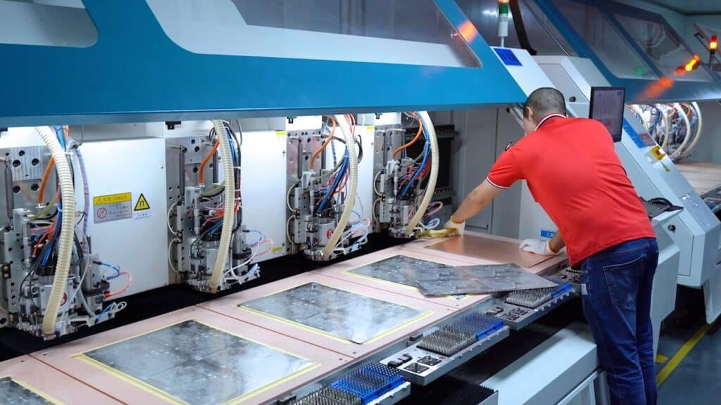
4. Lamination
Once the inner layers are patterned, they are stacked with prepreg sheets and outer copper foils in a specific order according to the design stackup. The stack is subjected to high temperature and pressure in a lamination press, bonding the layers into a single, solid board. This process ensures strong adhesion and precise alignment of layers, which is critical for maintaining electrical connectivity and structural integrity.
5. Drilling and Via Formation
Holes, known as vias, are drilled into the laminated board to create electrical connections between layers. These include through-hole vias (spanning the entire board), blind vias (connecting outer to inner layers), and buried vias (connecting inner layers only). Advanced laser drilling is often used for microvias in high-density interconnect (HDI) designs. The drilled holes are then plated with copper to establish conductive pathways, ensuring reliable interlayer connections.
6. Outer Layer Processing
The outer layers undergo a similar patterning and etching process as the inner layers to form the surface circuit patterns. A solder mask, typically green but available in other colors, is applied to protect the copper traces and prevent short circuits. A silkscreen layer is added to print component labels and identifiers for assembly. Finally, a surface finish (e.g., HASL, ENIG, Immersion Gold, or OSP) is applied to enhance solderability and protect exposed copper from oxidation.
7. Testing and Quality Assurance
Rigorous testing ensures the multilayer PCB meets design specifications and industry standards. Electrical tests, such as continuity and insulation resistance checks, verify connectivity and detect shorts or opens. Advanced inspection methods, including Automated Optical Inspection (AOI) and X-ray analysis, are used to check layer alignment, via integrity, and hidden defects. These tests are crucial for ensuring reliability in demanding applications like aerospace and medical electronics.
Why Choose JHYPCB for Multilayer PCB Manufacturing?
Selecting the right partner for multilayer PCB manufacturing is critical to ensuring the quality, reliability, and performance of your electronic products. JHYPCB stands out as a trusted manufacturer, offering advanced capabilities, rapid turnaround, and comprehensive services tailored to meet the needs of industries like telecommunications, automotive, and healthcare. With a focus on precision and customer satisfaction, JHYPCB delivers high-quality multilayer PCBs that support complex designs and cutting-edge applications. Below, we highlight the key reasons to choose JHYPCB for your multilayer PCB needs.
1. Comprehensive Manufacturing Capabilities
JHYPCB specializes in producing multilayer PCBs with 1 to 32 layers, catering to a wide range of applications. From HDI boards to high-TG, heavy copper, and flexible PCBs, our manufacturing capabilities cover diverse requirements. We support advanced features like blind and buried vias, high-frequency materials, and rigid-flex designs, ensuring your PCBs meet the demands of modern electronics, from IoT devices to aerospace systems.
2. Rapid Prototyping and Fast Delivery
Time-to-market is critical in today’s fast-paced electronics industry. JHYPCB offers rapid prototyping services, with expedited options as fast as 24 hours for single- and double-sided PCBs and 3–4 days for multilayer boards (4–8 layers). Our streamlined production process ensures low-volume orders are delivered in 5–7 days, while mass production for multilayer PCBs takes 10–12 days, depending on complexity. This flexibility helps you meet tight project deadlines without compromising quality.
3. Stringent Quality Assurance
Quality is at the core of JHYPCB’s manufacturing process. Our multilayer PCBs comply with industry standards such as IPC Class 3, RoHS, and ISO 9001:2008, ensuring reliability and performance. We employ advanced testing methods, including Automated Optical Inspection (AOI), X-ray analysis, and electrical testing, to verify layer alignment, via integrity, and circuit functionality. This rigorous quality control minimizes defects and ensures your PCBs perform flawlessly in critical applications.
4. Versatile Surface Finishes and Materials
JHYPCB offers a range of surface finishes to enhance solderability and protect your multilayer PCBs, including HASL, Lead-Free HASL, ENIG, Immersion Gold, Immersion Silver, Immersion Tin, and OSP. We also provide a variety of materials, such as FR4, high-TG substrates, and polyimide for flexible PCBs, to meet specific thermal, electrical, and mechanical requirements. This versatility ensures your boards are tailored to your application’s unique needs.
5. End-to-End PCB Solutions
Beyond manufacturing, JHYPCB provides turnkey PCB assembly services, including component sourcing, surface-mount technology (SMT), and through-hole assembly. Our one-stop approach simplifies your supply chain, reducing costs and lead times. Whether you need a quick prototype or large-scale production, our experienced team supports you from design to delivery, ensuring seamless project execution.
6. Global Reach and Customer Support
With a commitment to serving clients worldwide, JHYPCB offers fast, reliable shipping and responsive customer support. Our technical team provides expert guidance on design optimization, material selection, and manufacturing processes, helping you achieve the best results. Whether you’re developing a consumer gadget or an industrial IoT system, we partner with you to deliver high-quality multilayer PCBs that meet your specifications.
How to Choose the Right Number of Layers for Your Multilayer PCB
Choosing the right number of layers for a multilayer PCB is a critical decision that impacts performance, cost, and manufacturability. The layer count determines how complex a circuit you can design, how compact the board can be, and how much the production will cost. Whether you’re developing a smartphone, a medical device, or an industrial IoT system, selecting the optimal layer count requires balancing technical requirements with project constraints. Below, we outline the key factors to consider and provide guidance to help you make an informed choice for your multilayer PCB project.
1. Understand Your Circuit Complexity
The complexity of your circuit is the primary driver of layer count. Simple designs with basic functionality, like LED controllers, may suffice with single- or double-sided PCBs. However, applications requiring high-speed signals, multiple components, or intricate routing—such as 5G routers or automotive ADAS systems—often need multilayer PCBs. For example, a 4-layer PCB is common for consumer electronics like smartwatches, while high-performance servers or aerospace systems may require 12 or more layers to accommodate complex signal routing and power distribution.
2. Evaluate Space and Size Constraints
Multilayer PCBs allow you to pack more functionality into a smaller footprint by distributing circuits across multiple layers. If your project demands a compact design, such as a wearable device or a foldable smartphone, a multilayer PCB with 4–8 layers can reduce board size while maintaining performance. High-density interconnect technology, using microvias and fine traces, can further minimize layer count while achieving compact designs, which is ideal for space-constrained applications.
3. Consider Signal Integrity and Performance
High-frequency or high-speed applications, such as telecommunications equipment or data centers, require careful management of signal integrity. Multilayer PCBs with dedicated power and ground planes (typically starting at 4 layers) reduce electromagnetic interference (EMI) and improve signal quality. For example, a 6-layer PCB with separate ground and power layers ensures stable performance in 5G base stations. If your project involves high-speed signals or sensitive analog circuits, additional layers can enhance performance by providing better impedance control and reduced crosstalk.
4. Balance Cost and Budget
More layers increase manufacturing costs due to additional materials, complex processes, and extended fabrication time. A 4-layer PCB is often a cost-effective choice for consumer electronics, while 8–12 layers are justified for high-performance applications like medical imaging systems. To optimize costs, consider whether HDI technology can reduce layer count without sacrificing functionality. Early collaboration with your PCB manufacturer can help balance performance and budget by optimizing layer stackup and material choices.
5. Assess Manufacturing and Assembly Requirements
Higher layer counts require advanced manufacturing capabilities, such as precise layer alignment and microvia drilling, which may limit your choice of manufacturers. For instance, boards with 12+ layers or complex features like blind and buried vias demand specialized equipment and expertise. Ensure your project timeline aligns with the longer fabrication times of multilayer PCBs (e.g., 3–5 days for 4–8 layers, up to 10–12 days for 20+ layers). Discussing your design with a manufacturer early can help identify feasible layer counts based on their capabilities.
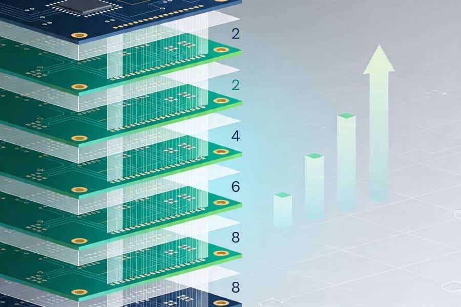
6. Typical Layer Counts for Common Applications
To guide your decision, here are common layer counts for various applications:
- 4–6 Layers: Consumer electronics (smartphones, tablets, smartwatches), IoT devices, basic automotive systems.
- 6–8 Layers: Telecommunications (routers, 5G modems), medical devices (diagnostic equipment), industrial controllers.
- 8–12 Layers: Advanced automotive (ADAS, EV battery management), servers, high-speed computing.
- 12+ Layers: Aerospace (avionics, radar), supercomputers, complex networking equipment.
By aligning your layer count with your application’s needs, you can optimize both performance and cost-effectiveness.
Cost Optimization Strategies for Multilayer PCBs
Multilayer PCBs offer unparalleled performance for complex electronics, but their higher manufacturing costs can be a concern for budget-conscious projects. By strategically optimizing design, materials, and production processes, you can significantly reduce costs without compromising quality or functionality. Whether you’re developing consumer electronics, automotive systems, or IoT devices, these cost optimization strategies will help you balance performance and budget. Below, we outline practical approaches to make multilayer PCB production more cost-effective.
1. Minimize Layer Count with High-Density Interconnect (HDI)
Reducing the number of layers is one of the most effective ways to lower multilayer PCB costs, as each additional layer increases material and processing expenses. High-density interconnect technology, using microvias and finer traces, allows you to achieve complex routing in fewer layers. For example, a 6-layer HDI PCB can often replace an 8-layer standard PCB, maintaining performance while cutting costs. Collaborate with your design team to evaluate whether HDI can meet your project’s needs with a reduced layer count.
2. Choose Cost-Effective Materials
Material selection significantly impacts multilayer PCB costs. Standard FR4 substrates are more affordable than high-TG or low-loss materials like PTFE or polyimide, which are often required for high-frequency or high-temperature applications. If your project doesn’t demand specialized performance (e.g., 5G or aerospace), opt for FR4 to lower costs. Similarly, choose cost-effective surface finishes like HASL instead of pricier options like ENIG or Immersion Gold, unless specific solderability or durability requirements apply.
3. Optimize Design for Manufacturability
Simplifying your PCB design can reduce manufacturing complexity and costs. Minimize the use of advanced features like blind or buried vias, which require specialized equipment and increase fabrication time. Design traces and spacing to standard tolerances (e.g., 5-mil traces instead of 3-mil) to avoid costly high-precision processes. Use design-for-manufacturability (DFM) guidelines, such as avoiding tight tolerances or excessive via types, to streamline production and reduce defect risks.
4. Leverage Batch Production
Producing multilayer PCBs in larger quantities can significantly lower the cost per unit. Batch production spreads setup costs (e.g., tooling, testing) across more boards, reducing the overall expense. For example, ordering 100 units instead of 10 can decrease costs by up to 30%, depending on the manufacturer’s pricing model. Plan your production schedule to consolidate orders, and discuss volume discounts with your PCB supplier to maximize savings.
5. Collaborate Early with Your Manufacturer
Engaging your PCB manufacturer during the design phase can help identify cost-saving opportunities. Manufacturers can suggest stackup configurations, material alternatives, or process optimizations to reduce expenses while meeting performance goals. For instance, they may recommend adjusting layer stackups to use standard core thicknesses or simplifying via structures to avoid costly laser drilling. Early collaboration also ensures your design aligns with the manufacturer’s capabilities, minimizing costly revisions.
6. Streamline Testing and Quality Assurance
While rigorous testing is essential for multilayer PCBs, excessive or redundant testing can inflate costs. Focus on essential tests like Automated Optical Inspection (AOI) and electrical continuity checks for standard applications, reserving advanced methods like X-ray inspection for high-reliability projects (e.g., aerospace or medical). Work with your manufacturer to tailor the testing plan to your project’s needs, ensuring quality without unnecessary expenses.
Key Design Considerations for Multilayer PCBs
Designing a multilayer PCB requires careful planning to ensure optimal performance, reliability, and manufacturability. Unlike single- or double-sided PCBs, multilayer PCBs involve complex layer stackups, high-density components, and advanced routing strategies. These boards power sophisticated applications like 5G telecommunications, medical devices, and automotive systems, where signal integrity and thermal stability are critical. Below, we outline key design considerations to help engineers create high-quality multilayer PCBs that meet project requirements while minimizing costly revisions.
1. Optimize Layer Stackup for Signal Integrity
A well-designed layer stackup is essential for maintaining signal integrity in multilayer PCBs. Dedicate inner layers to power and ground planes to reduce electromagnetic interference (EMI) and provide stable voltage distribution. For high-speed applications, such as 5G modems or servers, place signal layers adjacent to ground planes to minimize crosstalk and control impedance. Use CAD tools like Altium Designer or Cadence Allegro to simulate stackups and ensure consistent impedance (e.g., 50 ohms for RF signals) across layers.
2. Prioritize Impedance Control
Impedance control is critical for high-frequency signals in multilayer PCBs, such as those in telecommunications or radar systems. To achieve controlled impedance, carefully select dielectric materials (e.g., FR4 with specific dielectric constant) and calculate trace widths and spacing based on the target impedance. For example, a 4-layer PCB with a ground plane beneath a signal layer can maintain stable impedance for high-speed USB or HDMI signals. Collaborate with your manufacturer to verify stackup and material choices during the design phase.
3. Manage Thermal Performance
Multilayer PCBs often power high-performance devices that generate significant heat, such as electric vehicle controllers or data center processors. Use high-TG FR4 or metal-core substrates for better thermal resistance in high-temperature environments. Incorporate thermal vias to transfer heat from components to inner or outer layers. For dense designs, consider adding dedicated thermal layers or heat sinks to dissipate heat effectively, ensuring long-term reliability in applications like automotive or industrial IoT systems.
4. Optimize Via Design and Placement
Vias are critical for interlayer connectivity in multilayer PCBs, but their type and placement impact performance and cost. Use through-hole vias for simpler designs, while blind and buried vias or microvias (in HDI PCBs) are ideal for high-density applications like smartphones. Minimize via count to reduce manufacturing complexity and cost, and ensure proper via spacing to avoid signal interference. For high-frequency signals, use back-drilled vias to reduce stub effects and improve signal quality.
5. Mitigate Electromagnetic Interference (EMI)
EMI can degrade performance in multilayer PCBs, especially in RF or high-speed digital applications. Place ground planes strategically to shield signal layers and reduce noise. Route high-speed traces away from sensitive analog components to prevent crosstalk. Use stitching vias to connect ground planes across layers, creating a low-impedance path for return currents. For sensitive applications like medical imaging, consider adding shielding layers or EMI filters to enhance performance.
6. Follow Design for Manufacturability (DFM) Guidelines
Adhering to DFM guidelines ensures your multilayer PCB design is practical and cost-effective to produce. Use standard trace widths and spacing (e.g., 5-mil traces for standard processes) to avoid costly high-precision manufacturing. Ensure adequate clearance around vias and components to facilitate assembly. Provide clear Gerber files and stackup documentation to your manufacturer, and perform DFM checks using tools like Altium or KiCad to identify potential issues before production begins.
FAQs About Multilayer PCBs
Multilayer PCBs are a critical component in modern electronics, but their complexity often raises questions for designers, engineers, and procurement managers. To help you make informed decisions, we’ve compiled answers to some of the most frequently asked questions about multilayer PCBs. From layer counts to cost considerations, these FAQs address key aspects of their design, manufacturing, and applications.
Single-sided PCBs have components and circuits on one side only, making them suitable for simple, low-cost devices like LED lighting or basic controllers. Double-sided PCBs feature circuits on both sides connected through vias, offering more design flexibility for moderately complex applications like amplifiers or HVAC controllers. Multilayer PCBs, with three or more conductive layers laminated together, support far greater circuit complexity, higher component density and better signal integrity — making them essential for advanced electronics such as smartphones, 5G equipment, medical devices and automotive systems.
The right layer count depends on your circuit complexity, space constraints, signal integrity requirements and budget. As a general guide: 4–6 layers suit consumer electronics and IoT devices; 6–8 layers are common for telecom equipment, 5G modems and medical diagnostics; 8–12 layers serve high-performance computing, servers and advanced automotive systems (ADAS, EV battery management); 12+ layers are reserved for aerospace avionics, radar and supercomputing. When in doubt, consult your PCB manufacturer early — HDI technology can often achieve the same performance with fewer layers, reducing cost.
Several factors drive multilayer PCB cost: layer count (more layers = more material and processing); board size and quantity (larger panels and lower volumes cost more per unit); material choice (FR4 is more affordable than high-TG, PTFE or polyimide); via types (blind and buried vias require laser drilling, adding cost); surface finish (HASL is cheaper than ENIG or Immersion Gold); trace and spacing tolerances (tighter tolerances demand higher-precision processes); and lead time (expedited production carries a premium). Early DFM collaboration with your manufacturer is the most effective way to control costs.
Multilayer PCBs are significantly harder to repair than single- or double-sided boards. The hidden inner layers, dense component placement and fine trace geometries make fault diagnosis difficult without specialized equipment such as X-ray inspection systems. Minor surface-level repairs — like replacing a damaged SMD component or reflowing a solder joint — are generally feasible. However, inner layer defects, delamination or broken buried vias are often not repairable in the field. In mission-critical applications (aerospace, medical), a defective board is typically replaced rather than reworked to ensure reliability.
Multilayer PCBs are used across virtually every advanced technology sector. The industries that benefit most include: telecommunications (5G base stations, routers, satellite systems); automotive (ADAS, EV battery management, infotainment); healthcare (MRI, CT scanners, pacemakers, wearable monitors); aerospace and defense (avionics, radar, military communications); consumer electronics (smartphones, tablets, wearables); and industrial IoT and automation (smart factory sensors, robotics, PLCs). Any application requiring high component density, reliable signal integrity and compact form factor is well suited to multilayer PCB technology.
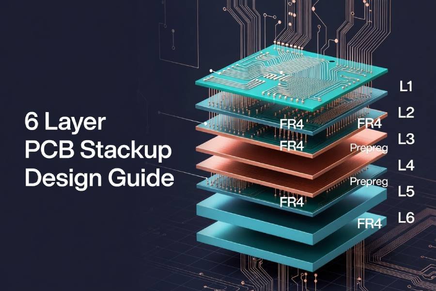
A 4-layer PCB is the most common type of multilayer PCB, consisting of four conductive copper layers: typically two signal layers (top and bottom) and two inner layers dedicated to power and ground planes. This stackup significantly improves signal integrity and reduces electromagnetic interference (EMI) compared to double-sided boards. 4-layer PCBs are widely used in consumer electronics, IoT devices, basic automotive systems and industrial controllers. They offer a strong balance of performance, design flexibility and cost — making them the preferred starting point when a double-sided board is no longer sufficient.
You should consider a multilayer PCB when your design exceeds the routing capacity of a double-sided board, requires dedicated power and ground planes for better signal integrity, demands a compact footprint with high component density, or operates at high speeds or frequencies where EMI control is critical. Common triggers include: the need to route complex mixed-signal circuits, integration of high-speed interfaces (USB 3.0, PCIe, DDR, 5G RF), space-constrained form factors (wearables, medical implants), or operation in demanding environments (automotive, industrial, aerospace).
3-layer PCBs are theoretically possible but almost never manufactured in practice, for two main reasons. First, a stackup with an odd number of layers is asymmetric — the uneven stress distribution during lamination causes the board to warp or bow, making it unreliable and difficult to assemble. Second, there is no practical routing or cost advantage over a 4-layer board: the most common 3-layer configuration (two signal layers + one plane) still requires the same lamination process as a 4-layer board, at similar cost. Manufacturers therefore skip directly from 2-layer to 4-layer designs.
Not necessarily. More layers provide greater routing flexibility, better signal integrity and more dedicated power/ground planes — but they also increase cost, fabrication time and design complexity. The optimal layer count is the minimum needed to meet your project's electrical, thermal and density requirements. Over-specifying layers wastes budget; under-specifying creates signal integrity or routing problems. HDI technology can often achieve high-density routing in fewer layers, offering a better cost-performance balance. Always design for the layer count your application genuinely requires, and consult your manufacturer to validate the stackup before committing.
Standard multilayer PCB thickness is 1.6 mm (0.063 inches), which is the most common specification for 4–8 layer boards and suits the majority of consumer and industrial applications. However, total thickness varies depending on layer count, core and prepreg material thickness, and copper weight. Thinner boards (0.8 mm or 1.0 mm) are used in compact devices like wearables and smartphones; thicker boards (2.0 mm or more) are found in heavy-duty industrial and automotive applications. Always confirm your thickness requirements with your PCB manufacturer, as stackup design directly affects both board thickness and signal integrity performance.
Conclusion
Multilayer PCBs are the backbone of modern electronics — from the smartphone in your pocket to the 5G base station on the rooftop, from electric vehicle controllers to life-saving medical implants. Their ability to combine high circuit density, superior signal integrity, compact form factor and long-term reliability in a single laminated stackup makes them indispensable wherever performance and space both matter.
As this guide has shown, the key to a successful multilayer PCB project lies in making the right decisions early: choosing the correct layer count for your circuit complexity, selecting materials suited to your operating environment, designing with signal integrity and thermal management in mind, and optimizing your stackup for both performance and cost. Whether you are working with a 4-layer consumer IoT board or a 20-layer HDI design for aerospace, these fundamentals apply across the board.
If you are ready to move from design to production, JHYPCB offers full-cycle multilayer PCB manufacturing from 1 to 32 layers — including HDI, rigid-flex, high-TG and heavy copper options — with rapid prototyping in as fast as 24–72 hours and rigorous IPC Class 3 quality assurance. Our engineering team can review your Gerber files, suggest stackup optimizations and provide a DFM-checked quote to help you get your boards right the first time.
Upload your Gerber files or send your requirements to sales@pcbjhy.com and our team will respond within 24 hours.