Table of Contents
Introduction to Copper Core PCB Stackup
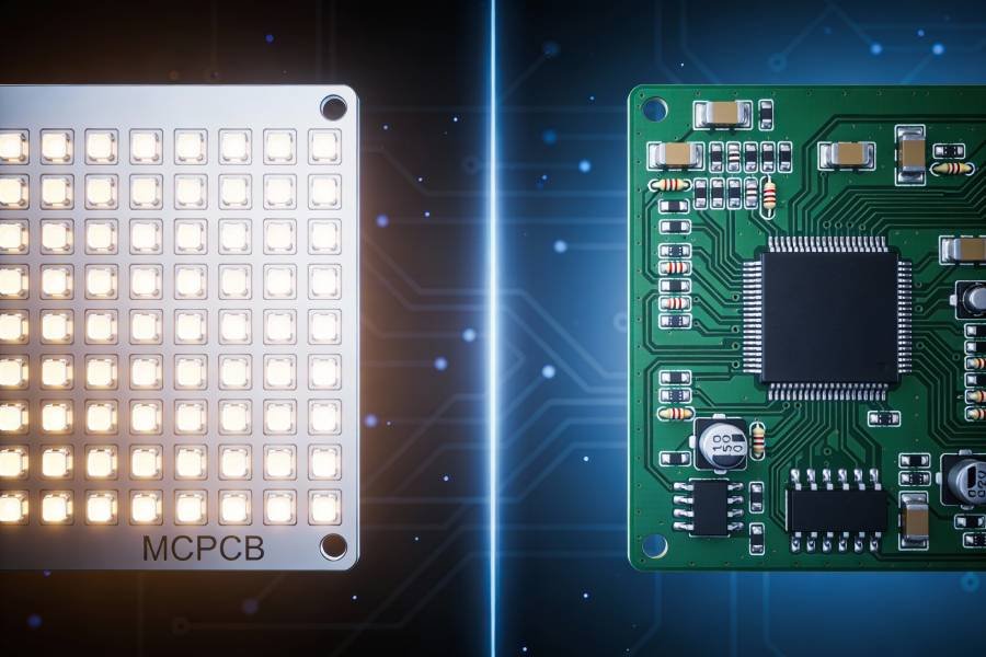
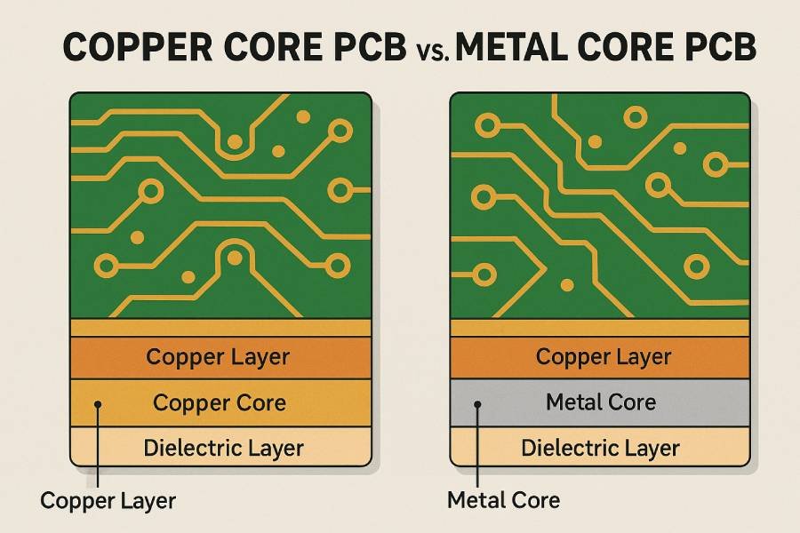
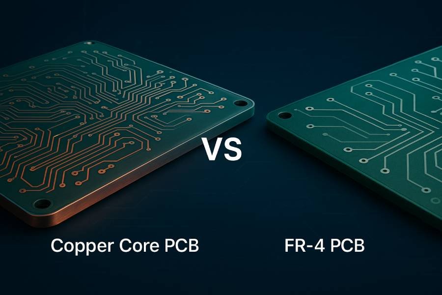
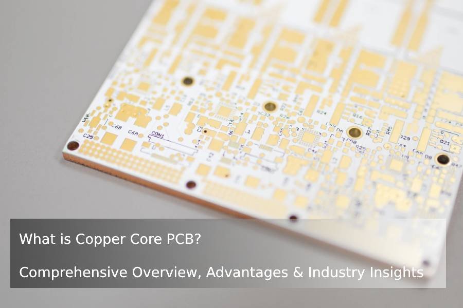
Copper core PCBs are rapidly becoming a vital component in today’s electronics industry, especially within applications where heat management and reliability are mission-critical. Unlike traditional FR-4 or ceramic boards, a copper core PCB features a solid copper plate embedded within the substrate, serving as an efficient heat conductor and structural backbone.
But why is stackup configuration so important?
Stackup refers to the arrangement and layering of materials—including copper layers, dielectrics, and the copper core itself—within the PCB. The way these layers are structured directly impacts the board’s thermal performance, electrical behavior, mechanical stability, and overall manufacturability. A well-optimized stackup not only ensures that heat is efficiently dissipated from components, but also preserves signal integrity and reduces the risks of warping or delamination.
For engineers, designers, and procurement specialists, understanding copper core PCB stackup is essential for maximizing the benefits of this advanced technology. In the following sections, we’ll explore how to select materials, configure layers, and design your PCB to achieve superior thermal and reliability performance—ensuring your products meet the toughest requirements in power electronics, automotive, industrial automation, and beyond.
Core Benefits of Optimized Copper Core PCB Stackup
Optimizing the stackup of a copper core PCB unlocks significant performance improvements and ensures your design can handle the demands of modern electronic applications. Here are the key benefits of a well-designed copper core PCB stackup:
1. Superior Thermal Management
The embedded copper core acts as an efficient heat sink, rapidly absorbing and spreading heat away from hotspots such as power devices or high-brightness LEDs. This capability allows electronic components to run cooler, improves system reliability, and can enable designers to push the power envelope without risking thermal failure.
2. Enhanced Electrical Performance
A carefully constructed stackup improves signal integrity by minimizing crosstalk and controlling impedance. The copper core’s high conductivity stabilizes voltage references and ground planes, making it ideal for circuits operating at high frequencies or sensitive analog signals where signal noise must be minimized.
3. Mechanical Stability and Durability
Copper is robust and dimensionally stable, giving the PCB inherent mechanical strength. An optimized stackup reduces the risk of warping, delamination, or cracking—especially important for boards subject to repeated thermal cycling or mechanical stress.
4. Extended Product Lifespan
Better thermal dissipation and mechanical resilience combine to protect electronic components and solder joints, preventing early failure and significantly extending product lifetime in harsh environments.
5. Miniaturization and Design Flexibility
With improved heat management, designers can pack more functionality into smaller form factors, enabling compact, lightweight, and higher-density boards without sacrificing performance.
In summary, the advantages of copper core PCB stackup go far beyond raw heat conduction—they improve every critical aspect of electronic reliability and performance. When designed with care, the stackup is a foundational pillar for successful products in industries such as automotive, power supplies, industrial automation, and advanced lighting.
Key Stackup Design Considerations for Copper Core PCBs
Designing the stackup for a copper core PCB calls for thoughtful choices and a clear understanding of how each material and layer affects the board’s performance. Below are the critical considerations that influence effective stackup design:
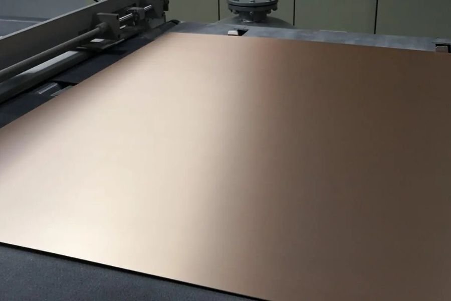
1. Copper Core Thickness and Material Selection
The copper core is the heart of the stackup—its thickness and purity directly impact both thermal conductivity and mechanical strength. Thicker copper enhances heat transfer and stability, but also makes drilling and processing more challenging. Typically, designers choose copper thickness based on the anticipated thermal load and physical constraints of the final application. For demanding power electronics, a core thickness ranging from 1mm to several millimeters is common.
2. Layer Arrangement and Configuration
The stackup arrangement defines how signal, power, and ground layers interact with the copper core. Options vary from simple two-layer boards for basic applications to advanced multilayer stackups (e.g., 4-layer or 6-layer designs) for complex systems:
2-layer structure: surface copper – dielectric – copper core – dielectric – surface copper
4-layer structure: signal layer – prepreg – power plane – copper core – ground plane – prepreg – signal layer
More layers mean greater routing flexibility and improved performance, but also increase complexity and cost.
3. Dielectric Material and Thickness
Dielectric layers sit above and below the copper core, serving as electrical isolation and signal carriers. Engineers should select dielectrics based on their thermal conductivity, dielectric strength, and compatibility with the copper core. Thinner dielectrics offer better heat transfer but may result in reduced voltage isolation. Common options include FR-4, polyimide, and other high-performance thermoset materials.
4. Copper Weight and Distribution
Copper weight (measured in ounces per square foot) must be chosen according to current-carrying needs and thermal requirements. Heavy copper is ideal for power layers, while lighter copper suits signal routing. Uniform copper distribution across layers prevents mechanical stress, minimizes electrical imbalances, and maintains stackup stability.
5. Signal Integrity and Impedance Control
For high-frequency or sensitive analog circuits, controlling impedance in the stackup is vital. Use controlled dielectric thicknesses, smooth copper surfaces, and symmetrical layer arrangements to minimize signal loss and crosstalk.
6. Manufacturing Constraints
Stackup choices must align with your manufacturer’s capabilities. Factors like drill size, lamination pressure, and maximum board thickness can influence achievable layouts. Early communication with your PCB vendor helps avoid costly redesigns or production delays.
Successful copper core PCB stackup design is the result of balancing electrical, thermal, mechanical, and manufacturing requirements. By considering these elements early in the design process, you’ll create boards that are not only high-performing but also reliable and manufacturable.
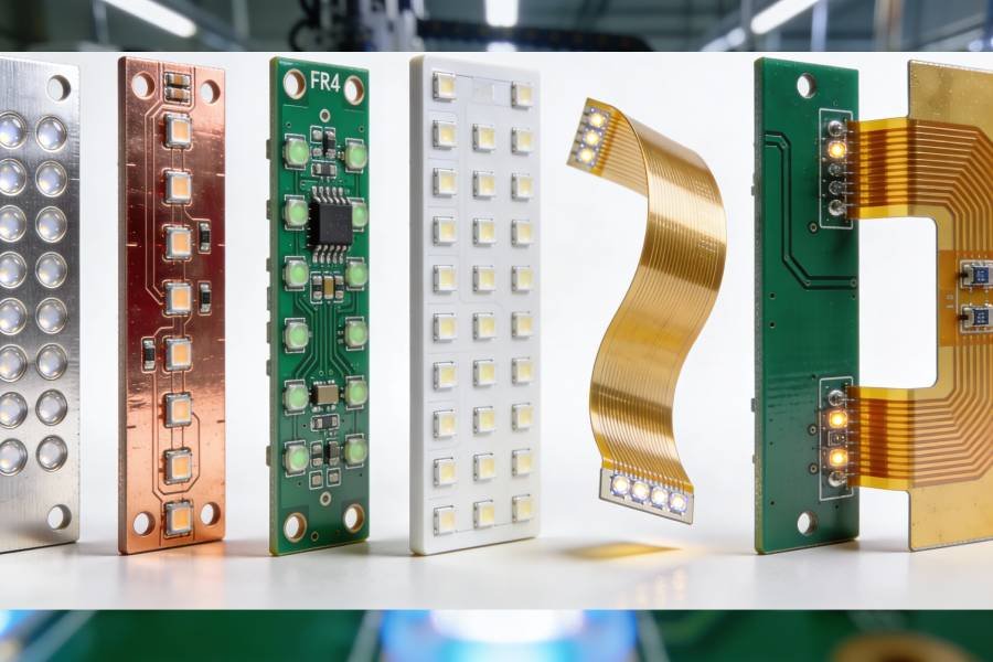
Common Copper Core PCB Stackup Configurations
A variety of stackup configurations are used in copper core PCB designs, each serving different functional and thermal requirements. Understanding these configurations will help you select or specify the optimal layout for your application.
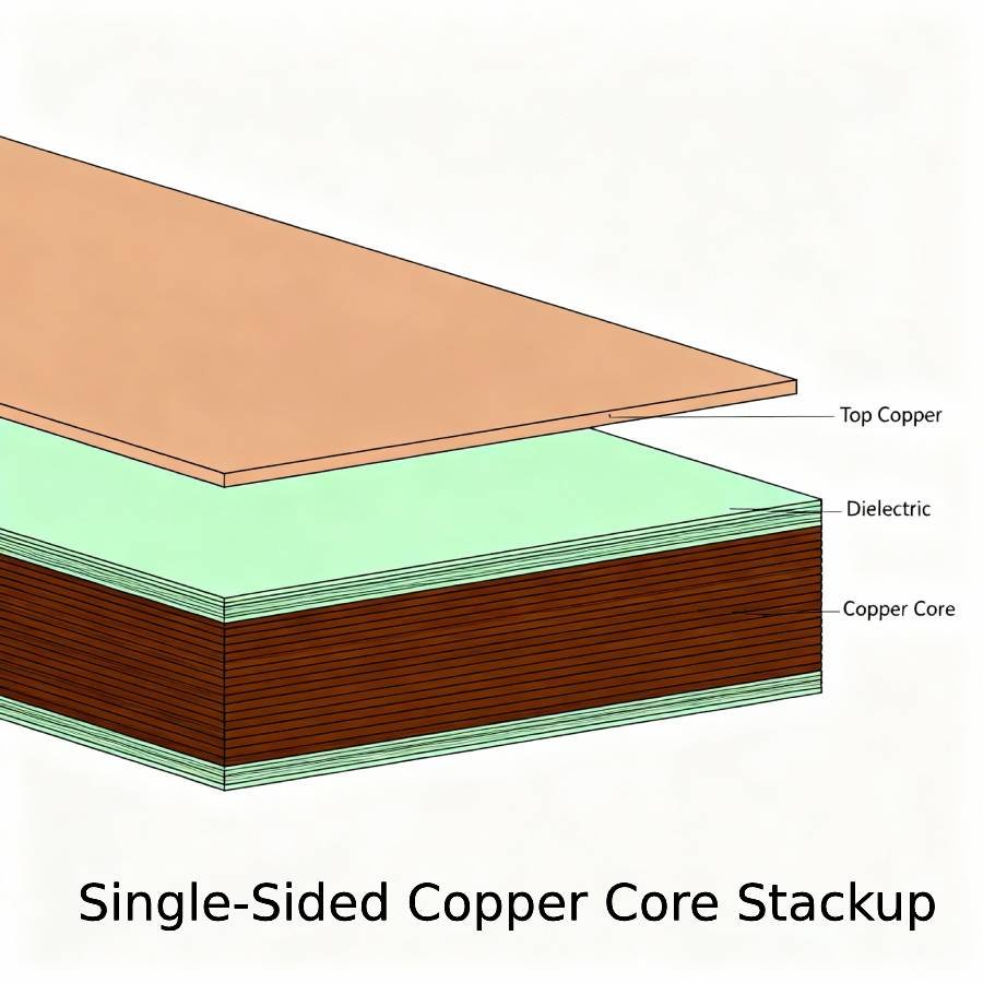
Single-Sided Copper Core Stackup
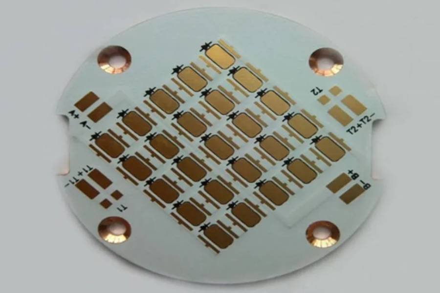
This basic arrangement features conductive traces on one side (top), with the copper core directly beneath the circuit layer. It’s ideal for simple, high-current applications such as power modules and basic LED lighting where efficient heat conduction is a priority and design complexity is minimal.
Typical structure:
Top Copper (Signal Layer) → Dielectric → Copper Core
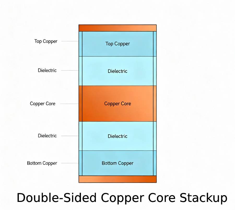
Double-Sided Copper Core Stackup
Double-sided stackups add a copper or conductive layer on both the top and bottom sides of the board, providing routing flexibility and supporting more complex circuit designs. This configuration is well suited to densely packed LED modules and automotive power devices.
Typical structure:
Top Copper (Signal Layer) → Dielectric → Copper Core → Dielectric → Bottom Copper (Signal Layer)
Multilayer Copper Core Stackup
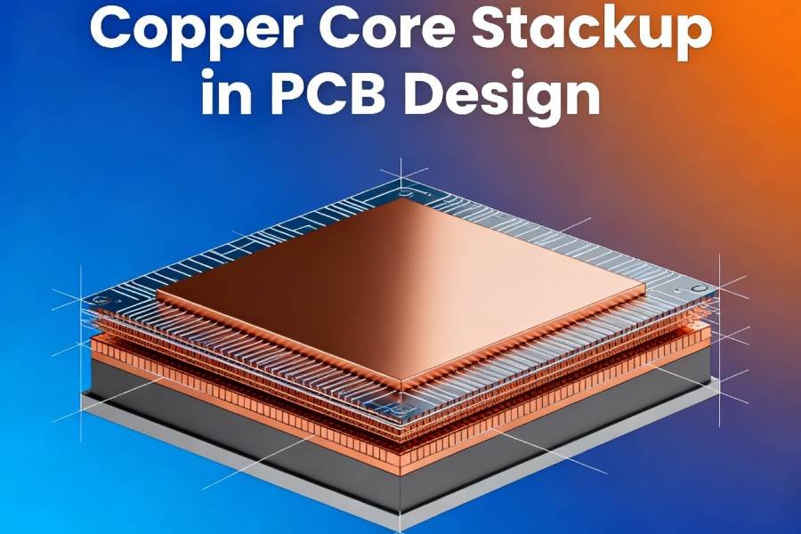
For advanced electronics that require both high power and signal integrity, multilayer designs are favored. Common configurations include 4-layer and 6-layer stackups. These structures allow for separated signal, power, and ground planes, as well as thermal management strategies such as internal copper pours and dedicated thermal/via planes.
Example: 4-Layer Copper Core Stackup
Top Signal Layer
Prepreg/Dielectric
Inner Power or Ground Plane
Copper Core
Inner Power or Ground Plane
Prepreg/Dielectric
Bottom Signal Layer
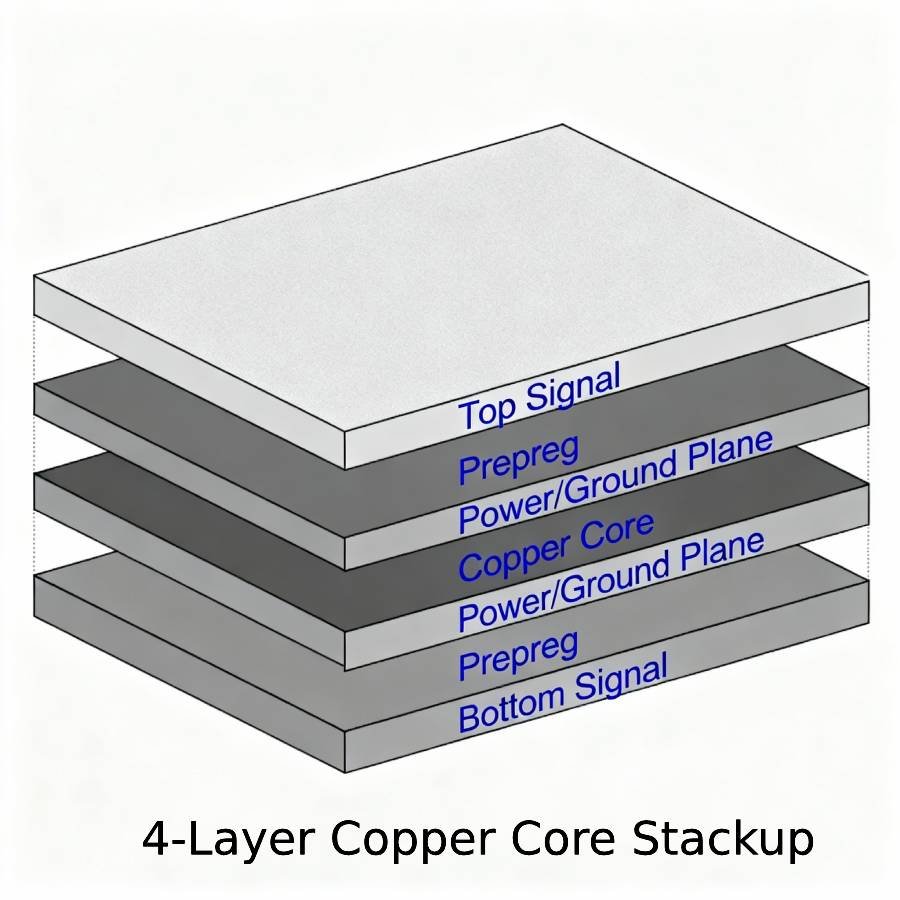
Key Features of Multilayer Stackups:
Thermal conduction is efficiently routed from internal heat sources to the copper core.
Signal quality is preserved using dedicated ground and power planes.
Mechanical strength is heightened, supporting demanding application environments.
Case Study: Power LED Module
Powerful LED lighting modules often employ a 4-layer copper core stackup. In this configuration, thermal vias transfer heat from the LEDs through the dielectric and into the copper core, while ground and power planes stabilize voltage and reduce electrical noise. The result: LEDs run cooler, last longer, and provide consistent light output.
Visual Aids
Consider including diagrams or exploded views of the above stackup configurations in your blog post. Visuals help readers (especially engineers and designers) better understand material layering and design logic.
Selecting the right copper core PCB stackup configuration is a strategic decision that should reflect your project’s performance, thermal, and reliability needs. Whether you require the simplicity of a single-sided board or the advanced capabilities of a multilayer layout, optimizing your stackup is essential for electronic success.
Thermal Management Strategies in Copper Core Stackup
Effective thermal management is one of the main reasons engineers choose copper core PCBs. The stackup structure plays a decisive role in how well a board dissipates heat and maintains optimal operating temperatures for sensitive components. Here’s how to maximize thermal performance with your copper core PCB stackup:
1. Via Design for Heat Dissipation
Thermal vias—vertical conductive holes connecting surface pads directly to the copper core—allow heat to flow from components into the core quickly. Strategic placement and adequate quantity of these vias ensure efficient heat extraction from high-power devices, such as MOSFETs, LEDs, or voltage regulators.
2. Integrating Thermal Pads and Heat Sinks
Thermal interface pads placed above the copper core, sometimes combined with external heat sinks, help to create a low-resistance thermal path. By positioning critical components directly above these pads, you enable the copper core to serve as the primary heat spreader, reducing temperature rise and enhancing system reliability.
3. Copper Pours and Plane Layers
Large copper pours—expanses of copper linked to ground, power, or thermal networks—help to distribute and absorb heat across the PCB. Design your stackup so these pours connect efficiently to the copper core and to vias, maximizing the area available for thermal conductivity.
4. Optimal Dielectric Selection
Choosing dielectric materials with high thermal conductivity further accelerates heat transfer from components and traces to the copper core. Materials like ceramic-filled epoxies or advanced polyimide blends can improve overall PCB thermal performance.
5. Balancing Electrical and Thermal Needs
Designing for thermal management should not come at the expense of signal integrity or electrical isolation. Ensure your layout keeps adequate spacing between thermal vias, pours, and signal paths to prevent electrical shorts or impedance issues.
Practical Tip:
Always simulate the thermal performance of your stackup using PCB design software. This allows you to predict hotspots, verify cooling efficiency, and avoid thermal failures before prototyping.
Your copper core PCB stackup is the foundation of effective thermal management. By leveraging vias, thermal pads, optimized copper pours, and high-conductivity dielectrics, you ensure that heat is rapidly removed from electronic components—extending product life and preventing costly downtime or malfunctions.
Manufacturing Challenges and Solutions for Copper Core PCB Stackups
Copper core PCBs deliver exceptional benefits, but they also introduce unique manufacturing complexities that must be addressed to ensure consistent quality and performance. Recognizing potential challenges—then applying proven solutions—will make the difference between a reliable product and a costly setback.
1. Delamination and CTE Mismatch
One major risk is delamination, where layers separate due to differences in the coefficient of thermal expansion (CTE) between copper and dielectric materials. When the board experiences thermal cycling, stresses accumulate at the interfaces.
Solution:
Select dielectric materials compatible with the copper core’s CTE and use advanced bonding agents during lamination. Controlled lamination cycles and pressure are also crucial for strong adhesion.
2. Drilling and Plating Through Thick Copper
Drilling vias and through-holes in thick copper is more complex than in standard PCBs. There’s increased tool wear, potential for burrs, and difficulties in achieving consistent plating in deep, narrow holes.
Solution:
Utilize CNC equipment with specialized drill bits designed for hard metals. Employ step drilling and optimized parameters to reduce burrs. Enhance plating processes with pulse plating or advanced electrolytic baths for reliable, even copper distribution inside vias and holes.
3. Warping and Dimensional Stability
Large copper cores can cause warping during lamination and cooling, especially if copper thickness isn’t balanced or the stackup lacks mechanical symmetry.
Solution:
Design stackups with balanced copper weights and symmetrical layer structures. Perform pre-production thermal and mechanical simulations to anticipate and mitigate warpage risks.
4. Lamination and Material Compatibility
Bonding copper to dielectric materials requires precise control of temperature, pressure, and lamination time. Inadequate control can lead to weak bonds and board failure.
Solution:
Work closely with experienced PCB manufacturers who understand copper core processes. Use only certified materials and tightly monitored, automated lamination equipment to ensure repeatable, high-quality results.
5. Design for Manufacturability (DFM) Issues
Complex stackups with high layer counts or unusual geometries may exceed a manufacturer’s production limits or require special handling.
Solution:
Involve your manufacturer early in the design process. Share stackup details, layer count, thicknesses, and anticipated production volumes to confirm manufacturability and avoid delays.
Copper core PCB stackups demand advanced manufacturing skills, precise machinery, and deep technical knowledge. By proactively addressing each challenge—CTE management, drilling and plating, warping, lamination, and manufacturability—you set your project up for successful production, lower defect rates, and consistent end-use performance. Partnering with a specialized manufacturer like JHYPCB ensures that these complex processes are handled professionally, delivering reliability at scale.
Best Practices for Engineers and Designers
To make the most of copper core PCB stackups, it’s vital for engineers and designers to adhere to best practices that streamline development, facilitate manufacturing, and guarantee performance. Here’s what to keep in mind:
1. Follow Manufacturer’s DFM (Design for Manufacturability) Guidelines
Consult with your PCB manufacturer early and often, sharing draft stackups and critical specifications. Manufacturers can recommend copper weights, minimum/maximum layer thicknesses, and suitable materials based on their equipment and expertise. Leveraging their DFM checklists prevents costly design errors and ensures your stackup is viable for mass production.
2. Prioritize Copper Balancing and Symmetry
Balanced copper distribution on either side of the copper core prevents warping and improves dimensional stability during lamination and thermal cycling. Aim for symmetrical layer structures whenever possible, especially in multilayer boards.
3. Maintain Adequate Clearances and Robust Thermal Reliefs
Respect minimum copper-to-edge, copper-to-hole, and copper-to-component clearances as specified by your manufacturer. For thermal management, design robust thermal relief structures—such as spokes around pads—to improve solderability without compromising heat flow.
4. Use Controlled Impedance and Proper Trace Planning
For high-speed signals, incorporate controlled impedance traces and maintain consistent dielectric spacing. Use reference ground planes adjacent to signal layers and avoid unnecessary layer transitions to minimize signal reflection and loss.
5. Simulate and Validate Your Stackup Early
Employ PCB design software to simulate electrical and thermal properties of your intended stackup. Early simulation helps identify potential hotspots, impedance issues, or structural weaknesses so you can resolve them before prototyping.
6. Document Stackup Details Thoroughly
Provide comprehensive stackup drawings and documentation—including layer sequence, thicknesses, copper weights, dielectric constants, and material types—during the handoff to your manufacturer. Any ambiguity can result in production errors or delays.
7. Anticipate End-Use Requirements and Environment
Consider the operational environment of your board: Will it face wide temperature swings, vibration, or moisture? Design the stackup to match these demands, selecting materials and configurations for the specific application.
By following these best practices, engineers and designers maximize the benefits of copper core PCB stackups—ensuring manufacturability, robust thermal performance, and reliable operation. Close collaboration with your manufacturer, diligent simulation, and precise documentation are the pillars of a successful copper core PCB project.
Conclusion
Optimizing the stackup configuration of copper core PCBs is essential for unlocking their full potential in modern electronics. By thoughtfully selecting materials, balancing copper distribution, and designing with both thermal and electrical performance in mind, engineers and manufacturers can create boards that exceed expectations for reliability, efficiency, and longevity.
A well-designed copper core PCB stackup not only dissipates heat more effectively but also preserves signal integrity and mechanical strength, making it a top choice for demanding applications in automotive electronics, industrial automation, power supplies, and advanced lighting systems. When you follow best practices—such as collaborating closely with experienced manufacturers, running early design simulations, and documenting every detail—you lay the foundation for a robust project with minimal risk of costly revisions or performance issues.
As the electronics industry continues to push the boundaries of miniaturization and power density, copper core PCBs and their optimized stackups stand out as game-changing solutions. For businesses seeking competitive advantage and long-term reliability, investing in the right stackup design isn’t just a technical decision—it’s a strategic one.
Ready to achieve maximum performance from your copper core PCB projects? Consult with JHYPCB’s team of experts to get tailored stackup guidance and professional manufacturing support, ensuring your next product is both powerful and dependable.