Table of Contents
Introduction
In every new generation of electronic products, there is a clear trend toward devices that are thinner, lighter, and more intelligent, yet packed with far more functionality than before. Flexible printed circuit boards (flex PCBs or FPCs) have become one of the key technologies that make this combination of miniaturization and high performance possible. Instead of relying only on rigid FR‑4 boards and bulky wiring harnesses, designers now route signals through bendable circuits that can fold, twist, and wrap around three‑dimensional structures.
A flexible PCB is built on a thin, bendable polymer film—typically polyimide or polyester—rather than on a stiff glass‑epoxy substrate. This flexible base layer carries fine copper traces and is covered by a protective coverlay, forming a circuit that can withstand repeated bending without losing its electrical integrity. By replacing multiple rigid boards, connectors, and cables with a single integrated flex or rigid‑flex assembly, engineers can significantly reduce weight, volume, and the number of potential failure points in the system.
Today, flex PCBs are widely used in smartphones, cameras, wearables, medical sensors, automotive modules, aerospace systems, and many other products where space is tight and reliability is critical. They enable camera modules to fold into ultra‑slim devices, allow medical patches to conform to the human body, and help automotive electronics survive continuous vibration and temperature cycling. For design teams, learning when and how to use flexible PCBs has become a core competency rather than a niche skill.
In this article, JHYPCB will explain what a flexible PCB is in detail, walk through its main types and materials, highlight essential design guidelines, outline the manufacturing process, and share typical applications and reliability considerations. The goal is to provide a practical, engineering‑oriented guide that helps you decide whether flex or rigid‑flex technology is the right choice for your next project.
What Is a Flexible PCB?
A flexible printed circuit board (flex PCB, FPC, or flexible circuit) is a type of PCB built on a bendable insulating film instead of a rigid glass‑epoxy substrate. In practical terms, it is an electrical circuit that can bend, fold, or twist while maintaining stable electrical performance and mechanical integrity. This combination of electrical functionality and mechanical flexibility makes flex PCBs an ideal interconnection technology for compact, three‑dimensional, and dynamically moving assemblies.
In a traditional rigid PCB, copper traces are etched on a stiff FR‑4 core, and the board is designed to remain flat throughout its life. A flexible PCB uses a thin polymer film—typically polyimide (PI) or polyester (PET)—as the base material, with copper conductors laminated on one or both sides and protected by a flexible coverlay instead of a standard solder mask. Because the whole structure is thin and compliant, the circuit can conform to curved surfaces, pass through tight hinges, or wrap around mechanical features that would be impossible for a rigid board.
Functionally, a flex PCB still behaves like any other PCB: it routes power and signals between components and subsystems, can be impedance‑controlled, and can carry high‑speed interfaces or sensitive analog signals when properly designed. The difference lies in the mechanical behavior and the way the circuit is integrated into the product. Instead of using several rigid PCBs connected by cables and connectors, designers can often replace the entire harness with a single flex or rigid‑flex assembly, reducing weight, volume, connection count, and assembly time. This is why flexible circuits are increasingly used in wearables, medical patches, foldable devices, automotive camera modules, and many other applications where space is limited and motion or vibration is present.
In the next sections, this article will look more closely at how flexible PCBs are constructed, the main types you will encounter, key materials such as polyimide and rolled‑annealed copper, and the design and manufacturing considerations that distinguish flex and rigid‑flex boards from their rigid counterparts.
Structure and Types of Flexible PCBs
Basic Structure of a Flex PCB
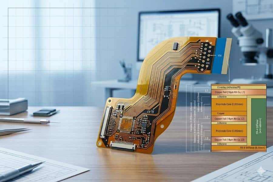
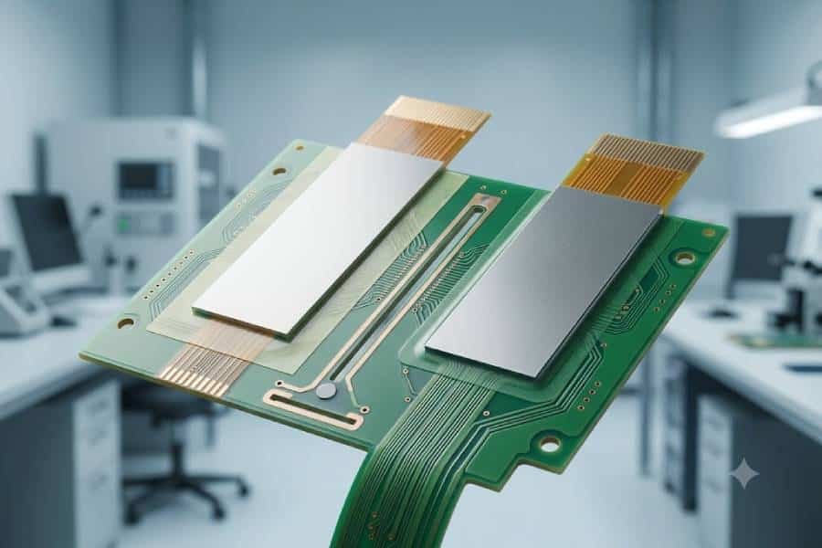
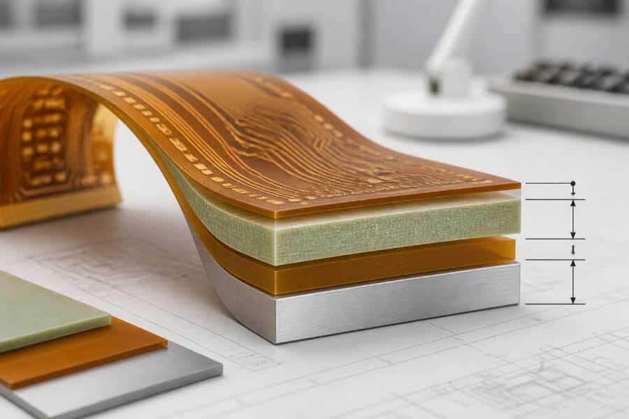
At a high level, the structure of a flexible PCB is similar to that of a rigid PCB, but every layer is chosen to allow bending and repeated flexing. A typical flex PCB stack‑up consists of a flexible base film, one or more copper layers, adhesive layers (in some constructions), and a protective coverlay that replaces the conventional solder mask. Together, these layers form a thin, robust laminate that can conform to complex three‑dimensional shapes without cracking.
The flexible base material is usually polyimide (PI) or polyester (PET), providing excellent bendability, heat resistance, and dimensional stability. Copper foil is laminated to this substrate and patterned into fine traces, while the coverlay—typically a polyimide film with adhesive—encapsulates the copper to protect it from moisture, chemicals, and mechanical damage. Depending on the design, additional elements such as stiffeners, shielding foils, and selective solder mask may be added in specific areas to support components, control impedance, or improve mechanical strength.
Single‑Sided Flexible PCBs
A single‑sided flexible PCB is the simplest form of flex circuit, with copper on only one side of the flexible substrate and a coverlay on top. The structure typically includes a polyimide base film, a single copper layer etched into the required circuit pattern, and a protective coverlay that leaves openings only where pads or fingers are needed for soldering or connection. Because there is only one conductor layer, there are no plated‑through vias within the flex area.
Single‑sided flex PCBs offer maximum flexibility, lowest cost, and straightforward manufacturing, making them ideal for simple interconnects, dynamic flexing applications, and high‑volume consumer products. Typical uses include printer head connections, simple display link cables, button or keypad tails, and internal jumpers where signal routing is not very complex.

Double‑Sided Flexible PCBs
Double‑sided flexible PCBs have copper layers on both sides of the flexible core and use plated‑through holes to connect traces between the two sides. The stack‑up usually consists of a flexible base film, copper on each side, and coverlay applied to both outer surfaces, with drilled and plated vias providing vertical interconnections. This configuration greatly increases routing freedom compared with single‑sided designs while still maintaining good flexibility.
By using both sides of the flex, designers can cross signals, integrate more complex circuits, and place pads or contact fingers on either side where needed. Double‑sided flex PCBs are widely used in devices that need moderate circuit density and frequent bending, such as cameras, foldable consumer products, automotive sub‑assemblies, and medical devices where space is limited but the circuitry is more involved than simple jumpers.

Multilayer Flexible PCBs
Multilayer flexible PCBs stack three or more copper layers separated by flexible dielectric films, allowing sophisticated routing, controlled impedance, and integrated power or ground planes within a fully flexible construction. The stack‑up can include a combination of signal layers, reference planes, and shielding layers, all built on polyimide with carefully engineered thickness and adhesive systems to manage bending stress. Plated‑through, blind, and buried vias may be used to connect different layers, similar to multilayer rigid boards but executed with flexible materials.
These multilayer flex circuits are used when high interconnect density, noise control, and compact packaging must be combined with the ability to bend or fold the assembly. Typical applications include high‑end camera modules, compact control units, aerospace and defense electronics, and complex medical or industrial sensors where multiple subsystems are connected within a tight mechanical envelope. Compared with single‑ or double‑sided flex, multilayer designs require more careful attention to stack‑up symmetry, copper balancing, and bend radius to avoid reliability issues.

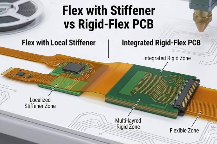
Rigid‑Flex PCBs
Rigid‑flex PCBs combine rigid sections and flexible sections into a single integrated structure, using one or more flex layers to interconnect rigid PCB areas. In a typical rigid‑flex construction, flexible polyimide layers run through or between rigid FR‑4 sections, and plated‑through holes provide continuous interconnection across both rigid and flexible regions. This approach allows designers to mount components on rigid areas for mechanical support while using the flex portions only where bending or folding is necessary.
Rigid‑flex technology is especially attractive when multiple rigid boards would otherwise need to be connected with cables and connectors. By integrating everything into a single rigid‑flex assembly, engineers can reduce connector count, improve signal integrity, save space and weight, and enhance reliability under vibration or thermal cycling. Common use cases include smartphones and tablets, aerospace and military systems, medical implants and diagnostic equipment, and advanced automotive electronics where packaging constraints are severe. Later sections of this guide will explore design and manufacturing aspects that are unique to rigid‑flex compared with pure flex or pure rigid solutions.
Key Materials Used in Flexible PCBs
Flexible Base Films: PI, PET and Others
The foundation of any flexible PCB is its base film, which provides mechanical support, electrical insulation, and the ability to bend without cracking. The two most common flexible substrates are polyimide (PI) and polyester (PET), with polyimide being the dominant choice in high‑reliability electronics.
Polyimide films offer excellent thermal stability, mechanical strength, and dielectric properties over a wide temperature range. They can withstand soldering temperatures, repeated flexing, and harsh environments, making them ideal for dynamic flex applications, multilayer flex circuits, and rigid‑flex boards used in automotive, aerospace, medical, and industrial systems. PET films, in contrast, support lower temperature operation and have more limited flex endurance, but they are cost‑effective and well‑suited for static or mildly flexed circuits in consumer products, transparent LED modules, and disposable devices.
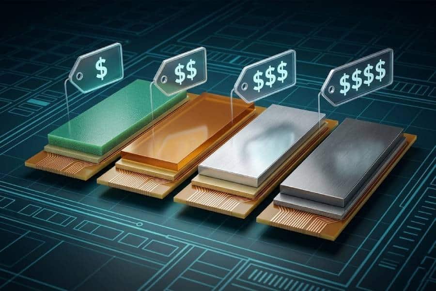
In addition to PI and PET, some designs use PEN or specialized high‑frequency films to meet specific requirements for signal integrity, chemical resistance, or ultra‑thin constructions. The substrate choice directly impacts bend radius, long‑term reliability, and cost, so it is critical to match the film type and thickness to the mechanical and environmental conditions of the final product.
Copper Foil: RA vs. ED Copper
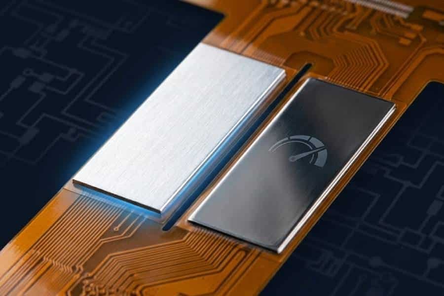
Copper foil is the primary conductor material in flexible PCBs and is typically supplied as either rolled‑annealed (RA) or electro‑deposited (ED) copper. RA copper is mechanically worked and annealed to create a fine, elongated grain structure that offers superior ductility and bending endurance, while ED copper is plated from solution and tends to be more columnar and less flexible. This microstructural difference has a direct influence on how well the copper can tolerate repeated flexing.
For flex circuits that will bend frequently or dynamically during use—such as hinges in foldable devices, moving cable replacements, or rigid‑flex layers subjected to vibration—RA copper is generally preferred because it can survive many more flex cycles before cracking. ED copper is often used in static or limited‑flex applications, as well as in thick‑copper constructions where cost and higher current capacity are more important than maximum bend life. In many rigid‑flex designs, the flexible layers specifically call for RA copper to ensure long‑term reliability, while ED copper may be used in purely rigid sections.
Adhesive vs. Adhesiveless Constructions
Between the copper and the base film, flexible circuits can be built using either adhesive‑based or adhesiveless laminates. In adhesive‑based constructions, a thin layer of epoxy or acrylic adhesive bonds the copper foil to the polyimide film, creating a three‑layer structure that is relatively easy to manufacture and cost‑effective. However, the adhesive layer adds thickness, can reduce bend performance, and may be a point of weakness under high temperature or aggressive chemical exposure.
Adhesiveless laminates, by contrast, bond copper directly to the polyimide without a separate glue layer, resulting in a thinner, more flexible, and more thermally stable stack‑up. These materials are widely used in high‑density, high‑reliability, or ultra‑thin flex and rigid‑flex boards found in aerospace, automotive, and advanced consumer electronics. The choice between adhesive and adhesiveless systems involves trade‑offs among cost, flexibility, processing requirements, and reliability targets, and it should be made early in the design stage in collaboration with the fabricator.
Coverlay and Protective Coatings
Instead of using a conventional liquid solder mask like rigid PCBs, flexible circuits typically rely on a coverlay—a flexible insulating film laminated over the copper to protect it. A standard coverlay consists of a polyimide film plus adhesive, with openings defined where pads, fingers, or test points must remain exposed for soldering or connection. This layer shields the copper from moisture, dust, abrasion, and chemicals while preserving the board’s ability to bend.
Coverlay materials are available in various thicknesses and constructions, including adhesiveless polyimide systems and alternative coatings such as flexible epoxy covercoats or PET‑based films for cost‑sensitive designs. Thinner, high‑temperature polyimide coverlays are preferred for demanding flex and rigid‑flex applications that require tight bend radii and high reliability, while thicker or more economical options can be used where flexibility demands are modest. Proper selection of coverlay thickness, adhesive type, and opening design is essential to avoid stress concentrations, pad lifting, and cracking in the bend regions.
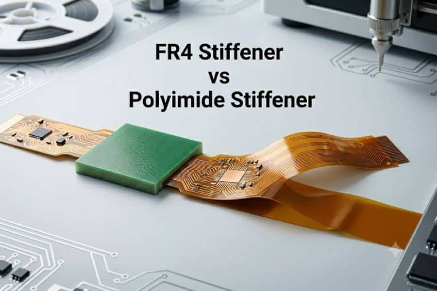
Stiffeners, Shielding and Other Auxiliary Materials
To support components, connectors, or mechanical interfaces, many flexible PCBs incorporate stiffeners made from FR‑4, polyimide, or stainless steel attached to local areas. These stiffeners create rigid zones where components can be reliably soldered and where connectors can withstand insertion and extraction forces, while the rest of the circuit remains flexible. In addition, copper or conductive films may be added as shielding layers or ground planes to improve EMC performance and signal integrity in high‑speed designs.
Other auxiliary materials include pressure‑sensitive adhesives for assembly, selective solder mask or covercoat for fine‑pitch areas, and special thermal‑management films for high‑power applications. Together with the base film, copper foil, adhesives, and coverlay, these materials give designers a rich toolbox for optimizing mechanical behavior, electrical performance, and cost. In later sections, this guide will show how material choices interact with stack‑up planning, bend radius, and manufacturing process windows to achieve a robust flex or rigid‑flex design.
Benefits and Limitations of Flexible PCBs
Key Benefits of Flexible PCBs
Flexible PCBs provide design freedom that is difficult to achieve with traditional rigid boards and cable harnesses. They can bend, fold, and twist to follow complex 3D paths, allowing electronics to fit into tight or irregular spaces without sacrificing electrical performance. This capability is especially valuable in modern consumer, medical, and automotive products where form factor is a critical design constraint.
Because a single flex or rigid‑flex assembly can replace multiple rigid PCBs, connectors, and wire harnesses, the overall system can become lighter, thinner, and mechanically simpler. Fewer connectors and solder joints mean fewer potential failure points, improved signal integrity, and higher reliability under vibration, shock, and thermal cycling. At the same time, assembly becomes more efficient: instead of routing and tying cables, operators can install one pre‑formed flex assembly, reducing labor time and assembly errors.
Thermal and environmental performance can also improve when flex technology is used correctly. Thin flexible substrates and optimized copper distribution can enhance heat spreading and ventilation, while high‑temperature polymers such as polyimide are resistant to many chemicals and harsh conditions. For applications that require repeated motion—like hinges in foldable devices, wearable sensors, or moving sensor modules—flex circuits provide long‑term bend endurance that rigid boards and traditional cable assemblies cannot match.
Main Limitations and Challenges
These advantages come with several important trade‑offs that must be considered early in a project. Flexible and rigid‑flex PCBs generally cost more per unit area than conventional rigid boards due to specialized materials, more complex stack‑ups, and additional manufacturing steps. Design cycles can also be longer because engineers must respect bend radii, layer transitions, and coverlay openings, and work more closely with the fabricator to ensure manufacturability.
There are also size, layout, and component‑placement constraints that do not exist in the same way on rigid PCBs. Very large or very wide flex circuits can be difficult or uneconomical to fabricate, and components generally cannot be placed in active bend regions without risking solder joint fatigue or pad cracking. Handling is more delicate during assembly and rework, because thin flexible laminates are easier to crease, scratch, or over‑stress compared with rigid boards. Once a flex circuit is fully fabricated, design changes—especially in the bend areas—are often more difficult and costly to implement than simple modifications on a rigid PCB.
In practice, these limitations do not negate the value of flex technology, but they do mean that flexible PCBs are most effective when used where their strengths clearly outweigh their added cost and complexity. Later sections of this guide will show how to apply design rules, material selection, and stack‑up planning to maximize the benefits of flex and rigid‑flex while managing their practical challenges.
Essential Flex PCB Design Guidelines
Bend Radius and Flex Region Design
One of the most critical parameters in flexible PCB design is the bend radius, which defines how tightly the circuit can bend without damaging the copper or substrate. As a general rule of thumb, the minimum bend radius should be significantly larger than the total flex thickness; common guidelines are 10:1 or more for static bends and up to 100:1 or higher for dynamic bends, depending on layer count and material system. Exceeding these limits can lead to cracked traces, broken vias, or delamination, especially in multilayer constructions.
Designers should clearly define flex regions, keep them as thin and symmetric as possible, and avoid unnecessary changes in thickness along the bend. When multiple layers are required, it is good practice to place critical conductors near the neutral axis to minimize strain, and to distribute copper evenly to avoid stiff spots and stress concentrations. Documenting bend directions, radii, and flexing conditions on the fabrication drawings helps the manufacturer validate the design against realistic mechanical loads.

Routing, Vias, and Stack‑Up Practices
Trace routing in flex areas should minimize mechanical stress. Instead of sharp 90‑degree corners, designers should use smooth, curved traces or shallow angles so that stress is distributed along the conductor rather than concentrated at a single point. In multilayer flex regions, routing patterns should be staggered between layers to avoid stacking traces directly on top of each other, which can create stiff lines that do not bend uniformly and are more prone to cracking.
Vias should generally be kept out of active bend areas and away from rigid‑flex transition zones because plated barrels are particularly vulnerable to fatigue under repeated flexing. When vias in flex regions are unavoidable, they should be placed at a safe distance from the bend, use generous annular rings and teardrop pads, and be accompanied by a carefully verified minimum bend radius. Stack‑ups should favor adhesiveless laminates and thinner copper weights in flexing zones to improve bend endurance, while using thicker copper and additional layers only where routing density or current requirements justify them.
Mechanical Support, Stiffeners, and Assembly Considerations
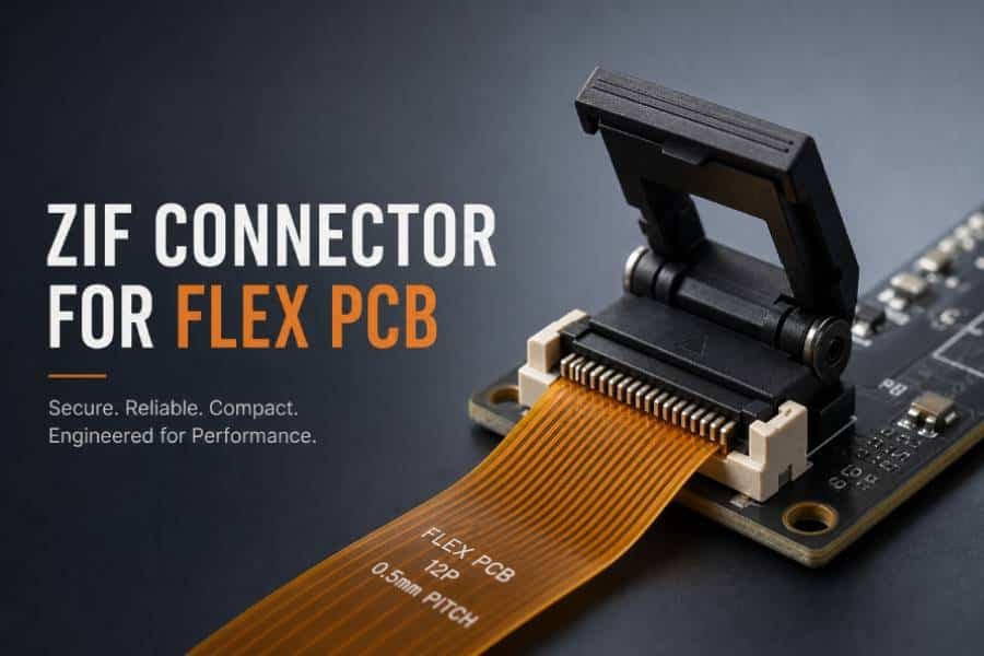
Because flexible circuits are thin and compliant, local mechanical reinforcement is often needed where components, connectors, or test points are located. Rigid or semi‑rigid stiffeners made from FR‑4, polyimide, stainless steel, or aluminum are commonly bonded to specific areas to provide thickness and support, allowing connectors to meet insertion‑force requirements and components to survive handling and assembly. The placement, material, and thickness of stiffeners should be coordinated with bend regions so that reinforcement does not unintentionally restrict required flexing.
During assembly, flex circuits must be handled carefully to avoid creasing, over‑bending, or pulling on unsupported component areas. Panelization, temporary carriers, and appropriate fixturing can help keep the flex portions flat during soldering and inspection, then allow the finished assembly to be folded into its final shape later. By considering mechanical support, connector specifications, and assembly processes early in the design, engineers can significantly reduce the risk of cracks, lifted pads, or intermittent connections in the finished product.
How Flexible PCBs Are Manufactured
From Raw Laminates to Circuit Patterns
The manufacturing of flexible PCBs starts with flexible laminates made from copper foil bonded to polyimide or other flexible films, using either adhesive or adhesiveless constructions depending on the design. These laminates are first cut into production panels and cleaned to remove any surface contamination that could affect imaging, plating, or adhesion. Because the materials are thin and easily damaged, handling and fixturing are more delicate than in rigid PCB production, and tension control on the production line becomes a key aspect of process stability.
Once the panels are prepared, drilling and via formation are carried out to create through‑holes and any required microvias, often using a combination of mechanical and laser drilling to suit the thin flexible stack‑up. The drilled holes are then desmeared, metallized, and plated with copper to form reliable interlayer connections. After via formation, the conductor pattern is created by applying photoresist, exposing the desired circuit image, and etching away unwanted copper, leaving behind the fine traces and pads that make up the flexible circuit.
Coverlay Lamination, Surface Finish and Profiling
Following circuit formation, a flexible coverlay or other protective coating is applied to encapsulate the copper and protect it from mechanical damage and environmental exposure. In a typical process, coverlay films with pre‑cut openings for pads and contact fingers are aligned and laminated to the flex panel under heat and pressure, allowing adhesive to flow and bond around the circuitry. Depending on design requirements, additional steps such as selective stiffener lamination, shielding layer attachment, or local solder mask application may be performed at this stage to prepare the assembly for component mounting.
The panels then receive a suitable surface finish—such as ENIG, immersion tin, or ENEPIG—on exposed copper features to ensure good solderability and corrosion resistance. Finally, the flexible circuits are routed, punched, laser‑cut, or otherwise profiled into their individual shapes, and electrical tests are performed to verify continuity and isolation. Throughout these steps, process controls for registration, dimensional stability, and handling are more stringent than for rigid boards, because even small misalignments or mechanical damage can compromise performance in thin, bendable structures.
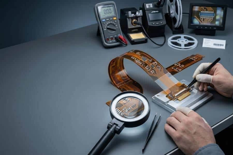
Assembly and Final Inspection of Flex PCBs
Assembly of flexible PCBs uses many of the same SMT and through‑hole processes as rigid boards, but usually with additional fixturing or carrier panels to keep the flex sections flat and stable during soldering. Components are placed and reflowed while the flex area is supported, and only after assembly and inspection is the circuit folded into its final three‑dimensional configuration. Rigid‑flex assemblies may be processed with some rigid sections acting as natural stiffeners, while pure flex designs often rely on temporary carriers that are removed after assembly.
Before shipment, finished flex and rigid‑flex boards undergo visual inspection, dimensional checks, and electrical testing to confirm that both the electrical performance and mechanical features meet specification. Particular attention is paid to coverlay registration, via plating quality, bend regions, and the integrity of stiffener bonds, since these areas are critical for long‑term reliability. When designers understand the key steps and sensitivities of flex PCB manufacturing, they can create stack‑ups and drawings that align with real process capabilities, improving yields and reducing the risk of late design changes.
Typical Applications of Flexible PCBs
Consumer Electronics and Mobile Devices
Flexible PCBs are deeply embedded in modern consumer electronics, especially smartphones, tablets, laptops, digital cameras, and wearable devices. They connect camera modules, buttons, sensors, speakers, and displays to the main logic board in extremely tight spaces, enabling slim designs, curved housings, and foldable or rotating form factors that would be difficult to achieve with only rigid boards and cables.
In smartphones and cameras, flex circuits route high‑speed signals between image sensors, lens assemblies, and processing boards, while accommodating moving parts such as zoom lenses or folding screens. Wearable devices like smartwatches and fitness trackers rely on flex PCBs to integrate batteries, sensors, antennas, and displays into thin, comfortable shapes that conform to the wrist or body, delivering reliability under constant motion and sweat or temperature changes.
Medical Devices and Wearable Healthcare
The medical sector uses flexible PCBs in both disposable and reusable devices, where small size, low weight, and patient comfort are critical. Flex circuits are found in hearing aids, implantable devices, diagnostic catheters, biosensors, and wearable patches that must conform closely to the human body while maintaining stable electrical performance. Their thin profiles and ability to bend without breaking are essential for routing signals in and around sensitive tissue.
Wearable medical monitors—such as ECG/EEG patches, continuous glucose monitors, and long‑term vital‑sign recorders—use rigid‑flex or pure flex architectures to connect flexible electrode arrays with rigid processing and battery modules. This approach allows devices to be lightweight, unobtrusive, and robust under daily activity, improving patient compliance and data quality for remote or continuous monitoring.
Automotive Electronics and Transportation
Automotive electronics are another major growth area for flexible and rigid‑flex PCBs. Inside vehicles, flex circuits are used in infotainment systems, instrument clusters, head‑up displays, steering‑wheel controls, seat modules, lighting assemblies, and various sensor systems where vibration, temperature cycling, and space limitations are significant challenges. Their ability to eliminate bulky wiring harnesses and multiple connectors helps reduce weight, simplify assembly, and improve long‑term reliability.
Rigid‑flex PCBs in particular are adopted for camera modules, radar and ADAS sensors, and advanced lighting or display units, where high‑speed signals must be routed through constrained mechanical paths. By integrating rigid logic boards with flexible interconnects, designers can meet stringent automotive standards for durability and EMC while keeping modules compact and serviceable.
Industrial, Aerospace, and Specialized Systems
In industrial automation, robotics, and instrumentation, flexible PCBs simplify connections in moving joints, compact control panels, and densely packed sensor arrays. They enable reliable signal routing in dynamic environments where cables would be prone to wear, snagging, or inconsistent performance, and they help reduce the size and complexity of control units, handheld tools, and measurement equipment.
Aerospace and defense systems make extensive use of rigid‑flex technology to achieve weight reduction, high reliability, and resistance to extreme conditions. Avionics modules, satellite electronics, UAV payloads, and mission‑critical control units use rigid‑flex assemblies to combine multiple rigid boards with flexible sections, eliminating connectors and harnesses while maintaining performance under vibration, shock, and wide temperature ranges. These same design principles are increasingly applied to other specialized fields, such as high‑end industrial sensors, quantum or scientific instruments, and ruggedized communication devices.
When to Choose Flex or Rigid‑Flex Instead of Rigid PCB
When a Rigid PCB Is Enough
Rigid PCBs remain the best choice for many designs where the board does not need to bend and where there is enough space for straightforward layouts and interconnects. They provide excellent mechanical support for components, are easy to fabricate in high layer counts, and usually offer the lowest cost per unit area, making them ideal for cost‑sensitive or structurally demanding products.
If a design can be implemented with standard board‑to‑board connectors or short cable assemblies without creating excessive complexity, bulk, or reliability risks, staying with rigid PCBs is often the most economical route. Rigid boards are particularly suitable when high power dissipation, large components, or stringent mechanical stiffness requirements dominate the design, and there is no need for the PCB itself to conform to curved or moving structures.
When to Use a Pure Flex PCB
A pure flex PCB is the preferred solution when the interconnection itself must bend, fold, or move repeatedly during operation, or when available space is so constrained that traditional rigid boards and cables cannot be packaged effectively. Typical triggers for choosing flex include the need to route circuits through hinges, rotating joints, tight channels, or around complex mechanical features while minimizing weight and thickness.
Designers should also consider flex when high reliability under vibration or motion is more important than minimizing PCB material cost. By replacing discrete wire harnesses and connectors with a single flexible circuit, the design can achieve fewer interconnect points, improved signal integrity, and simplified assembly, which often offsets the higher per‑area price of flex materials and processing.
When Rigid‑Flex Is the Better Choice
Rigid‑flex PCBs are most attractive when a product needs both rigid mounting areas for components and flexible interconnects between them within one integrated structure. Instead of using multiple rigid boards connected by flex cables and connectors, a rigid‑flex design embeds the flexible layers inside and between the rigid sections, reducing part count, connector failures, and assembly complexity while enabling compact 3D layouts.
This approach is especially useful in high‑reliability applications such as aerospace, military, medical, and advanced automotive systems, where vibration, shock, and thermal cycling make connectors and long harnesses potential weak points. However, rigid‑flex comes with higher material and fabrication costs, as well as more complex design rules, so it is usually justified when the gains in reliability, space savings, or system‑level cost clearly outweigh the added PCB expense.
Practical Decision Guidelines for Designers
From a practical standpoint, designers can start by asking a few key questions:
- Does the circuit need to bend or move during installation or operation?
- Are there severe space, weight, or connector‑reliability constraints?
- Will replacing cables and multiple rigid boards reduce assembly cost or improve performance?
If the answer to most of these questions is “yes”, flex or rigid‑flex technology is likely worth considering; if the answer is mostly “no”, a conventional rigid‑only approach may remain the best option. In many real projects, a hybrid strategy is used: critical areas use flex or rigid‑flex to handle motion and tight packaging, while the rest of the system continues to rely on cost‑effective rigid boards. Later sections of this article will discuss common failure modes and reliability practices to support whichever architecture is ultimately chosen.
Common Failure Modes and How to Improve Reliability
Typical Failure Modes in Flex and Rigid‑Flex
Flexible PCBs experience some failure modes that are rare or less critical in rigid boards, mainly due to continuous bending, thin materials, and complex interfaces. One of the most common issues is conductor fracture in bend regions, where repeated flexing or excessive bend radius leads to copper fatigue and eventual cracking of traces or via barrels. These problems are particularly pronounced in dynamic applications such as wearable devices, foldable electronics, and robotic joints.
Another frequent problem is delamination or layer separation, where the copper, adhesive, and polyimide or coverlay layers lose adhesion under thermal cycling, moisture, or mechanical stress. Delamination can manifest as bubbles, wrinkles, or local lifting around pads, in flex‑to‑rigid transition areas, or near stiffeners, and it may progress to open circuits or intermittent failures. Additional issues include pad lifting, solder joint cracking in bend‑adjacent component areas, insulation breakdown due to contamination or moisture, and wear or thinning of copper in high‑cycle flex regions.
Design‑Level Strategies for Higher Reliability
Many of these failures can be mitigated through thoughtful design before the first prototype is ever built. At the layout level, using generous bend radii, avoiding sharp trace corners, keeping vias out of active bend areas, and filleting pad‑to‑trace junctions all help to reduce stress concentrations that can initiate cracks. Placing critical conductors near the neutral axis, balancing copper across layers, and minimizing thickness changes within flex regions further lowers the strain imposed during bending.
Material and stack‑up choices also play a major role. Selecting RA copper for dynamic flex areas, using adhesiveless laminates for improved bend endurance, and specifying high‑temperature, high‑adhesion coverlay systems can significantly extend the life of a flex or rigid‑flex assembly. Clear documentation of bend conditions—number of cycles, direction, radius—and coordination with the fabricator allow appropriate design margins and process controls to be put in place, reducing the risk of surprises between prototype and production.
Process, Testing, and Assembly Best Practices
Reliability is also influenced by how flex circuits are manufactured, assembled, and tested. Tight control of lamination parameters, thorough pre‑baking to remove moisture, and proper storage conditions help prevent voids, poor adhesion, and moisture‑induced delamination in service. During assembly, using support fixtures or temporary carriers to keep flex sections flat, avoiding excessive handling stress, and keeping components away from active bend lines reduce the likelihood of pad lifting and solder joint cracks.
Finally, reliability testing tailored to flex applications—such as bend‑cycle tests, dynamic flex fatigue, thermal cycling, and combined stress testing—provides feedback on whether the design and materials are robust enough for the intended environment. By integrating these tests into the qualification plan and learning from early failures, design teams can refine geometries, stack‑ups, and process windows to deliver flexible circuits that perform reliably over the full life of the product.
How JHYPCB Supports Your Flex and Rigid‑Flex Projects
Engineering Support and DFM for Flex Designs
Successful flexible PCB designs require close collaboration between the design team and the manufacturer, especially around stack‑up planning, bend regions, and material selection. JHYPCB provides dedicated engineering and DFM support for flex and rigid‑flex projects, helping you verify that your bend radii, layer counts, copper weights, and coverlay openings are compatible with stable, high‑yield fabrication. This early review helps avoid costly redesigns, schedule slips, and reliability issues that can arise when flex rules are treated like ordinary rigid PCB rules.
Our engineers can review your Gerber files, stack‑up diagrams, and mechanical drawings to highlight potential risks—such as vias in bend areas, unbalanced copper, or overly aggressive thickness transitions—and suggest practical alternatives. For projects with tight packaging or demanding environments, JHYPCB can recommend suitable material systems, stiffener strategies, and panelization approaches, so that your design is manufacturable from the first prototype through to volume production.
Flexible PCB Manufacturing Capabilities at JHYPCB
As a full‑feature flexible PCB manufacturer, JHYPCB offers single‑layer, double‑sided, and multilayer flex circuits, as well as rigid‑flex boards that combine rigid and flexible sections into one structure. Our capabilities cover common polyimide‑based flex materials, RA and ED copper foils, adhesive and adhesiveless laminates, and a range of coverlay and surface‑finish options to meet different electrical, mechanical, and environmental requirements. These capabilities support both simple flex‑to‑install jumpers and complex high‑density interconnect designs.
JHYPCB serves customers in industries such as consumer electronics, automotive, aerospace, medical devices, and 5G communications, providing quick‑turn prototypes as well as small‑ and medium‑volume production with consistent quality. From fine‑line flex boards for compact devices to rigid‑flex assemblies for mission‑critical systems, our manufacturing processes are tuned for reliability, repeatability, and competitive lead times, allowing you to bring new products to market faster.
From Prototype to Production with JHYPCB
Most successful flex projects move through several prototype iterations before reaching stable production, and JHYPCB is equipped to support this full lifecycle. Rapid prototype runs let you validate fit, bend behavior, and assembly processes using the same materials and processes that will be used in volume, revealing manufacturability and reliability issues early. This approach reduces overall development risk and helps optimize stack‑ups, stiffener placement, and bend geometry before committing to large builds.
Once the design is proven, JHYPCB can seamlessly transition to higher‑volume manufacturing while maintaining the same process controls and quality standards. Whether you are developing a first‑generation wearable device, upgrading an automotive module to a rigid‑flex architecture, or adding flex interconnects to an existing system, JHYPCB aims to be a long‑term partner that supports you from initial concept through production and future product revisions. For detailed capability limits, quoting, or an engineering review of your current flex design, you can reach out directly via the JHYPCB website.
Key Takeaways and Next Steps
Flexible and rigid‑flex PCBs give designers powerful tools to solve problems of space, weight, and reliability that traditional rigid boards and cable harnesses struggle with. They enable compact 3D layouts, reduce connector count, and improve robustness in applications ranging from smartphones and wearables to medical, automotive, industrial, and aerospace systems. However, these benefits come with specific design rules, material choices, and manufacturing constraints that must be respected from the very beginning of the project.
For engineers and product teams, the most important habits are to plan realistic bend radii, choose appropriate materials (such as polyimide substrates and RA copper for dynamic flex), route carefully in bend regions, and work closely with an experienced flex manufacturer on stack‑up and DFM checks. Treating flex or rigid‑flex like a simple variant of rigid PCB design is one of the fastest ways to create fatigue, delamination, or assembly issues that only show up late in the development cycle.
If your next product must be thinner, lighter, or more mechanically integrated than the current generation, now is a good time to evaluate where flexible or rigid‑flex technology can replace cables, connectors, or extra rigid boards. By combining the guidelines in this article with early engagement from a manufacturing partner such as JHYPCB, teams can move from concept to reliable production flex designs with fewer iterations, better performance, and a clearer understanding of the trade‑offs involved.
Flexible PCB FAQs (Answered by JHYPCB Engineers)
For most static flex applications, a safe guideline is a minimum bend radius of at least 10 times the total flex thickness, while dynamic flexing may require 50–100 times depending on layer count and materials. Always confirm the final value with your manufacturer based on your exact stack‑up.
JHYPCB typically uses polyimide‑based laminates with RA or ED copper, combined with polyimide coverlay and optional stiffeners in FR‑4, PI, or stainless steel, selected according to your mechanical and environmental requirements. Alternative materials such as PET can be discussed for cost‑sensitive or special applications.
We accept standard PCB manufacturing formats such as Gerber (RS‑274X or X2), ODB++, IPC‑2581, and accompanying drill files, stack‑up notes, and mechanical drawings. Including clear bend region indications, stiffener outlines, and impedance requirements in your documentation helps us run a more accurate DFM review.
Yes, JHYPCB manufactures both pure flexible PCBs and rigid‑flex boards that integrate rigid sections with internal flex layers, supporting prototypes and production for applications such as consumer devices, automotive modules, and industrial or aerospace electronics.
Standard flex PCB prototypes generally ship in several working days depending on layer count, material availability, and complexity, while mass‑production lead times are set according to order quantity and process flow. Urgent projects can often be supported with expedited service after engineering review and schedule confirmation.
To quote accurately, we need your design files, target quantity, layer count, material and thickness requirements, copper weight, surface finish, special tolerances, and any assembly or testing needs. If you also share the application type and bend conditions, our engineers can suggest more cost‑effective and reliable material and stack‑up options.
Yes, JHYPCB offers engineering and DFM review for all flex and rigid‑flex projects, checking bend radii, via placement, copper balancing, coverlay openings, stiffener design, and panelization before production. This review helps catch manufacturability and reliability risks early so your prototypes and production runs are more robust.
JHYPCB serves customers in Europe, North America, Asia‑Pacific, and other regions, shipping flex and rigid‑flex PCBs globally with appropriate packaging and documentation. Our team can work with your preferred incoterms and logistics options to meet project deadlines and compliance requirements.
Key limitations include higher cost per area compared with rigid boards, constraints on very large panel sizes, restricted component placement in bend regions, and stricter rules for vias and thickness transitions. Early collaboration with your flex manufacturer helps you balance these constraints against the benefits of weight reduction, reliability, and 3D packaging.