Table of Contents
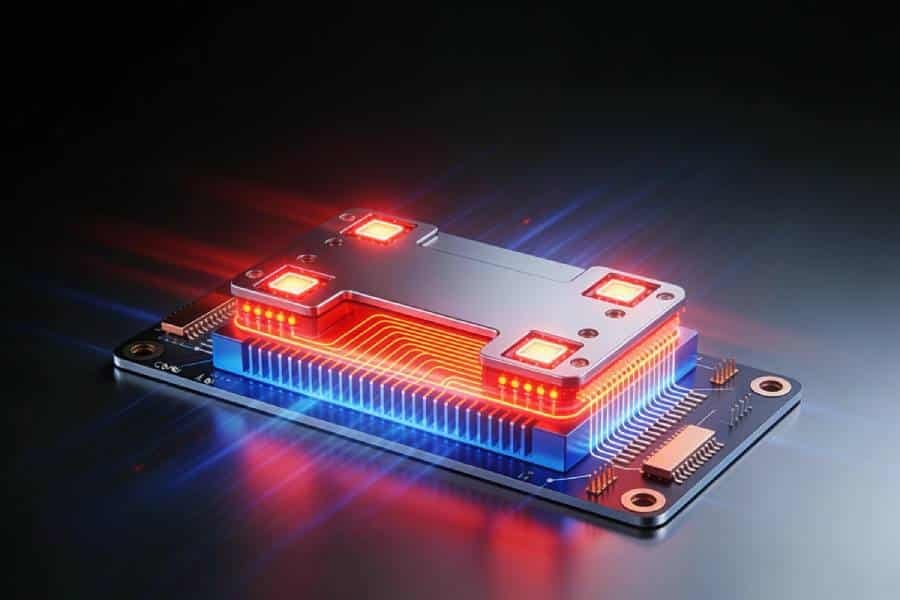
Introduction: Why Thermal Management is Critical for LED PCBs
LEDs transform electrical energy into light, but 60-80% of input power generates heat that must be efficiently dissipated to maintain performance, color consistency, and lifespan. Poor thermal management in LED PCBs causes junction temperatures to exceed safe limits, accelerating lumen depreciation, color shifting, and premature failures that undermine product reliability and brand reputation.
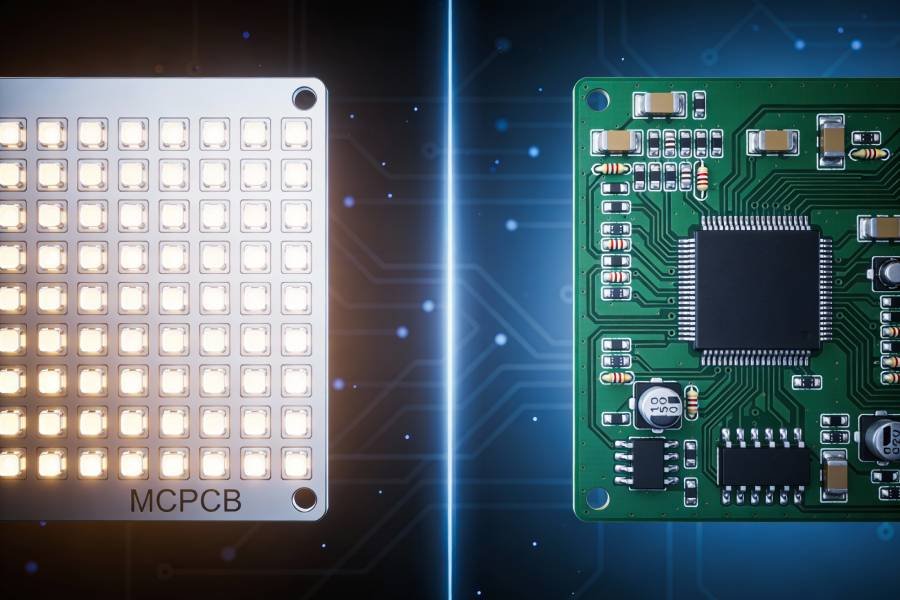
Aluminum LED PCBs and metal core PCBs (MCPCB) address these challenges through specialized materials and design strategies, but effective heat dissipation requires understanding thermal pathways from LED die through solder joints, copper traces, dielectric layers, and base metals to external heatsinks. Overheating not only reduces luminous efficacy by 10-20% per 10°C rise above 25°C, but also triggers failure modes like delamination, trace lifting, and solder fatigue in high-power applications.
This comprehensive guide dives deep into LED PCB thermal engineering, covering material thermal conductivity, PCB layout strategies, thermal vias, advanced MCPCB structures, interface materials, simulation tools, and validation testing. Engineers and designers will learn proven techniques to keep LED junction temperatures below critical thresholds, while procurement teams gain insights for evaluating LED PCB manufacturers with genuine thermal expertise. Mastering these principles ensures longer-lasting, higher-performing LED lighting systems across streetlights, automotive, displays, and industrial applications.
For projects that require both robust thermal design and stable production, partnering with a professional LED PCB manufacturing service can help you turn optimized thermal layouts into reliable aluminum LED PCB products at scale.
Understanding LED Heat Generation and Thermal Pathways
LEDs convert only 20-40% of electrical energy into light; the remaining 60-80% generates heat at the semiconductor p-n junction, creating the primary thermal challenge for LED PCB design. Effective thermal management requires tracing heat flow from LED die through multiple interfaces to ambient air, with each layer adding thermal resistance that elevates junction temperature (Tj).
1 LED Heat Generation Mechanisms
- Junction Heat Source: Electroluminescence produces photons, but non-radiative recombination and carrier leakage generate heat directly at the LED chip’s active layer.
- Phosphor Conversion Heat: White LEDs using blue chip + yellow phosphor create additional heat during wavelength conversion, contributing 15-25% of total thermal load.
- Driver Efficiency Losses: Constant current LED drivers contribute secondary heating through switching losses and voltage drops across series-connected LED strings.
2 Primary Thermal Resistance Path (Rth)
Heat flows sequentially through critical interfaces, each characterized by thermal resistance (Rth = ΔT/Q, measured in K/W):
LED Chip → Solder Joint → Copper Pad → PCB Traces → Dielectric Layer →

Metal Core/Base → TIM → Heatsink → Ambient Air
- Chip-to-Board (Rth-jb): Thermal resistance from junction to PCB surface, typically 3-10 K/W for SMD LEDs.
- Board-to-Core (Rth-bc): PCB dielectric layer represents the primary bottleneck in aluminum LED PCBs.
- Core-to-Ambient (Rth-ca): Metal base conduction to external heatsink via thermal interface material.
3 Thermal Bottlenecks by Application
| Application | Typical Tj Limit | Primary Heat Path Challenge |
|---|---|---|
| Indoor Lighting | 85°C | Dielectric layer Rth |
| Street Lighting | 100°C | High-power density |
| Automotive | 125°C | Vibration + thermal cycling |
| Display Backlights | 70°C | Uniformity across array |
Every 10°C rise above 25°C baseline degrades LED performance exponentially per Arrhenius equation:
Lumen Maintenance: Φv(Tj) = Φv(25°C) × e^(-k(Tj-25))

Color Shift: ΔCCT ≈ 100-200K per 20°C Tj increase

Lifespan: L70 ≈ L70_ref × e^(-Ea/k(Tj-Tref))
Maintaining Tj <85°C typically doubles LED lifespan from 30,000 to 60,000+ hours while preserving color consistency (Δu’v’ <0.003).
5 Heat Spreading vs Heat Extraction
- Spreading: Copper traces and planes laterally distribute heat from concentrated LED hotspots across larger PCB areas.
- Extraction: Metal cores (aluminum/copper) conduct heat vertically to external heatsinks or chassis.
- Convection: Final heat transfer to ambient relies on heatsink fin geometry, airflow velocity, and case-to-air thermal resistance.
Understanding these thermal pathways guides all subsequent LED PCB design decisions, from material selection through layout optimization. Each interface contributes cumulative resistance that compounds to determine final junction temperature and LED system reliability.
Thermal Properties of LED PCB Substrate Materials
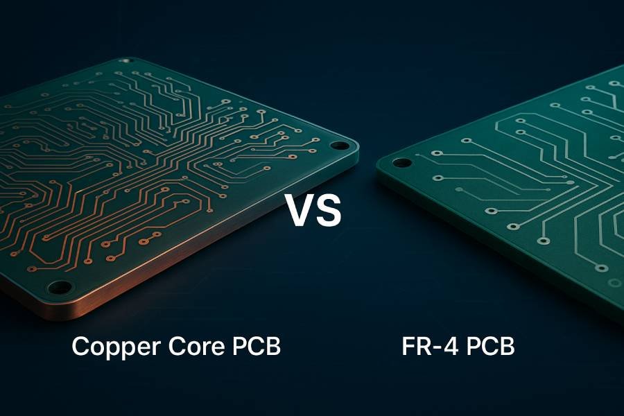
LED PCB substrate materials determine fundamental heat dissipation capability, with thermal conductivity (k, W/m·K), thickness, and CTE matching directly affecting junction temperatures and long-term reliability. Standard FR-4 fails high-power LED applications, making specialized metal core and ceramic substrates essential.
1 Common LED PCB Substrate Materials Comparison
| Material | Thermal Conductivity (W/m·K) | Thickness Range | Cost Index | Applications |
|---|---|---|---|---|
| FR-4 (std) | 0.25-0.3 | 0.4-3.2mm | 1x | Low-power indicators |
| Aluminum MCPCB | 1.0-4.0 (dielectric) | 1.0-3.0mm | 3-5x | Street lights, general lighting |
| High-Tg MCPCB | 6.0-8.0 | 1.5mm | 6-8x | Automotive, industrial |
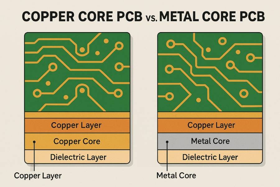
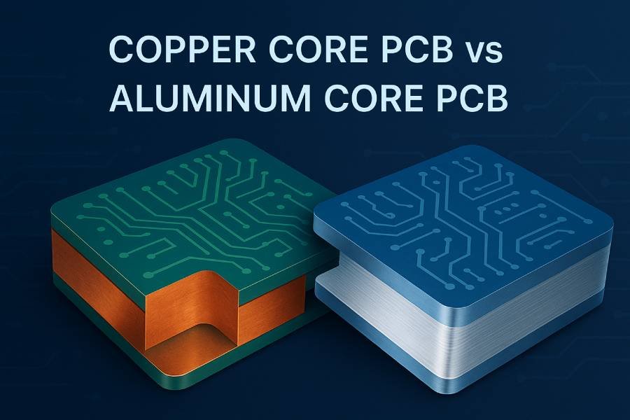
| Copper MCPCB | 3.0-6.0 | 1.5-2.0mm | 8-10x | High-power spotlights |
| Ceramic DBC | 20-30 (Al2O3), 170-230 (Cu) | 0.25-1.0mm | 15-25x | Laser diodes, aerospace |
Standard aluminum LED PCBs consist of three layers:
Copper Circuit (1-3oz) → Dielectric (1-3 W/m·K, 75-150µm) → Aluminum Base (1.0-2.0mm)
Thermal Resistance Equation: Rth = L/(k×A), where thinner dielectric dramatically reduces resistance:
- 100µm @ 1 W/m·K: Rth ≈ 1.0 K/W per cm²
- 150µm @ 3 W/m·K: Rth ≈ 0.5 K/W per cm²
3 Dielectric Layer: The Primary Thermal Bottleneck
Dielectric thickness creates exponential thermal resistance:
Rth ∝ thickness / thermal conductivity
- Standard dielectric (1 W/m·K, 100µm): Limits power density to <5 W/cm²
- High-performance dielectric (8 W/m·K, 75µm): Enables 15+ W/cm² for automotive headlights
4 CTE Matching and Reliability
Thermal expansion mismatch causes failures during temperature cycling:
α_aluminum = 22-24 ppm/°C α_copper = 17 ppm/°C α_FR4 = 12-18 ppm/°C
- Aluminum MCPCB dielectric must bridge 5-7 ppm/°C difference
- Ceramic substrates (6-8 ppm/°C) excel in extreme thermal cycling
5 Material Selection Guidelines by Power Density
- <1 W/cm²: Thick FR-4 with copper planes sufficient
- 1-5 W/cm²: 1.5mm aluminum MCPCB, 1-2 W/m·K dielectric
- 5-15 W/cm²: 1.5mm aluminum MCPCB, 4+ W/m·K dielectric + thermal vias
- >15 W/cm²: Copper MCPCB, embedded coins, or ceramic DBC
6 Cost vs Thermal Performance Trade-offs
Performance Gain:  Aluminum > Copper > Ceramic

Cost Scaling:       1x        3x        10x+
Sweet spot: 1.5mm aluminum MCPCB with 2-4 W/m·K dielectric delivers 80% ceramic performance at 20% cost.
Material selection establishes baseline thermal capability before PCB layout optimization. Aluminum MCPCB remains dominant for cost-effective high-power LED applications, balancing thermal conductivity, manufacturability, and mechanical robustness essential for long-term field reliability.
PCB Design Strategies for Heat Dissipation
Effective LED PCB layout transforms good substrate materials into optimal thermal performers. Strategic copper utilization, thermal via placement, and LED array geometry directly reduce junction temperatures by 20-40°C, extending lifespan and maintaining color consistency.
1 Copper Thickness and Heat Spreading Areas
Thicker copper lowers thermal resistance:
1oz (35µm): 140°C/W per cm²

2oz (70µm): 70°C/W per cm²

3oz (105µm): 47°C/W per cm²
- Solid copper planes under LED arrays spread heat laterally 3-5x more effectively than traces
- Minimum 2oz copper recommended for power densities >3 W/cm²
- Copper balancing: Equal copper weight on both sides prevents warpage in aluminum LED PCBs
2 Thermal Via Design and Optimization
Via array thermal resistance formula:
Rth_vias = (t_copper × ρ_copper) / (N × π × d²/4 × h_via)
Where N = number of vias, d = diameter, h = thickness
Optimal via parameters:
Diameter: 0.3-0.4mm (avoid <0.25mm)

Pitch: 1.0-1.5mm center-to-center

Fill: Uncapped or epoxy-filled (conductive fill +30% performance)

Density: 8-12 vias/cm² under high-power LEDs
Via plating: 25µm minimum copper to handle 5-10A peak currents
3 LED Placement and Thermal Isolation
Minimum spacing prevents thermal coupling:
Same-bin LEDs: 3-5mm edge-to-edge

Mixed-power: 6-8mm separation

High-power COB: 10mm clearance to adjacent SMDs
Staggered array patterns reduce hotspot formation:
Optimal: Hexagonal or diagonal layouts vs square grids

Airflow direction: Align LEDs perpendicular to flow
4 Multi-layer Thermal Design Strategies
4-layer aluminum LED PCB stack-up:
Layer 1: 2oz signal + LED pads

Layer 2: 1oz ground plane (thermal spreading)

Layer 3: 1oz power distribution

Layer 4: 2oz solid copper heat sink interface
Blind/buried vias connect surface copper directly to metal core, bypassing dielectric bottleneck.
5 Edge Effects and Board-Level Heat Distribution
Thermal shadowing: Keep >5mm copper-free border around board edges
Silkscreen avoidance: White legend reduces reflectivity by 10-15%
Mounting holes: 4-6mm diameter, plated through to core for chassis heat extraction
6 Design Rules Summary Table
| Parameter | Low Power (<1W) | Medium (1-5W) | High (>5W) |
|---|---|---|---|
| Copper oz | 1oz | 2oz | 3oz+ |
| Vias/cm² | None | 4-6 | 10-12 |
| LED Spacing | 2mm | 4mm | 6mm+ |
| Fill Type | None | Epoxy | Conductive |
| Ground Plane | Partial | Full | Full both sides |
FEA thermal analysis validates:
- Via array effectiveness (<5°C improvement target)
- Copper plane thickness justification
- LED spacing thermal crosstalk (<10°C Tj difference)
Iterative design: Start with conservative via density, thin copper; upgrade based on simulation confirming Tj <85°C under worst-case ambient + drive current.
These PCB-level strategies multiply substrate material performance by 2-3x. Combined with proper MCPCB selection, they maintain safe junction temperatures across demanding duty cycles while preserving luminous efficacy and color stability essential for commercial LED deployments.
Metal Core PCB (MCPCB) Thermal Engineering
Metal Core PCBs (MCPCBs) represent the gold standard for high-power LED thermal management, replacing FR-4’s poor heat spreading (0.3 W/m·K) with aluminum or copper bases offering 10-20x better conduction to external heatsinks. Understanding MCPCB layer interactions and dielectric optimization unlocks maximum thermal performance.
1 MCPCB Layer Structure and Heat Flow
Standard 3-layer construction:
Circuit Layer: 1-3oz Copper (35-105µm)

Dielectric: 75-150µm thermally conductive polymer (1-8 W/m·K)

Base: Aluminum (1.0-2.0mm, 220 W/m·K) or Copper (2.0mm, 400 W/m·K)
Primary heat path: LED pad → copper plane → dielectric → metal core → TIM → heatsink
Critical bottleneck: Dielectric layer contributes 60-80% of total Rth-jc despite thin profile.
2 Dielectric Thickness vs Thermal Resistance Trade-off
Rth_dielectric = t / (k × A)
Thickness impact:
- 75µm @ 2 W/m·K: Rth = 0.38 K/W·cm²
- 100µm @ 2 W/m·K: Rth = 0.50 K/W·cm²
- 150µm @ 4 W/m·K: Rth = 0.38 K/W·cm² (high-k solution)
Design rule: Target dielectric Rth <0.4 K/W·cm² for power densities >5 W/cm²
3 Single-Sided vs Double-Sided vs Multi-layer MCPCBs
| Type | Structure | Applications | Thermal Advantage |
|---|---|---|---|
| Single-sided | Cu-Diel-Al | Street lights | Simple, cost-effective |
| Double-sided | Cu-Diel-Al-Diel-Cu | Automotive | Both sides components |
| 4-6 layer | Hybrid Al/FR4 | Smart lighting | Signal integrity + thermal |
4 Aluminum Base Thickness Optimization
Thermal spreading radius ≈ √(4αt), where α = k/(ρCp)
Thickness guidelines:
- 1.0mm: Compact lights (<50W total)
- 1.5mm: Street lights (50-200W)
- 2.0mm: Industrial (>200W)
Warpage risk: Thinner cores (<1.2mm) require copper balance within 10% top/bottom.
5 Dielectric Material Performance Tiers
| Grade | k (W/m·K) | Thickness | Cost | Max Power Density |
|---|---|---|---|---|
| Standard | 1.0-2.0 | 100-150µm | $$ | 3-5 W/cm² |
| Performance | 3.0-5.0 | 75-100µm | $$$ | 8-12 W/cm² |
| Premium | 6.0-8.0 | 50-75µm | $$$$ | 15+ W/cm² |
Via-to-core connection: Plated vias transfer heat around dielectric barrier:
Optimal: 0.3mm dia., 12 vias/cm², uncapped or epoxy-filled

Rth_array ≈ 2-4 K/W for 1cm² hotspot
Avoid: Direct core contact (electrically unsafe) or overfilled conductive vias (short risk).
7 CTE Matching and Mechanical Reliability
Layer expansion rates:
Aluminum: 22-24 ppm/°C

Dielectric: 20-30 ppm/°C (optimized)

Copper: 17 ppm/°C
Fatigue life: Proper CTE matching survives 2000+ cycles (-40°C to 125°C)
8 MCPCB vs FR-4 + Heatsink Performance
Real-world comparison (10W LED array):
FR-4 + heatsink: Tj = 95°C @ Ta=40°C

1.5mm Al-MCPCB: Tj = 72°C @ Ta=40°C

Same heatsink, 23°C improvement
MCPCBs eliminate heatsink-to-board TIM interface while providing in-plane spreading, cutting junction temperatures 20-30°C versus traditional FR-4 solutions. Proper dielectric selection and via integration maximize this advantage for high-lumen, long-life LED deployments.
If you need engineering support and mass production for aluminum MCPCB and high‑power LED PCB designs, consider working with an experienced LED PCB manufacturer in China that specializes in LED PCB manufacturing and assembly.
Thermal Interface Materials (TIM) and Heat Sink Integration
The interface between LED PCB metal core and external heatsink represents the final thermal resistance barrier, often contributing 20-40% of total Rth-ca. Proper TIM selection, application pressure, and heatsink geometry optimization extract heat efficiently from aluminum LED PCBs to ambient air.
1 TIM Material Types and Performance Comparison
| TIM Type | Thermal Conductivity (W/m·K) | Bond Line Thickness (µm) | Applications | Cost |
|---|---|---|---|---|
| Thermal Grease | 1.0-8.0 | 20-50 | General lighting | $ |
| Phase Change | 3.0-6.0 | 50-100 | Automotive | $$ |
| Thermal Pads | 1.5-5.0 | 0.5-2.0mm | Easy assembly | $$ |
| Gap Filler | 2.0-6.0 | 1.0-5.0mm | Large gaps | $$$ |
| Indium Solder | 80+ | <50 | Extreme power | $$$$ |
Pads: No pump-out, but thicker bond lines increase resistance
2 Optimal Bond Line Thickness (BLT)
Rth_TIM = t_BL / (k_TIM × A)
Target: <50µm for grease, <0.5mm for pads
Example: 1W/cm², 25µm grease @ 4 W/m·K → Rth = 0.06 K/W·cm²

Same power, 1mm pad @ 2 W/m·K → Rth = 0.50 K/W·cm² (8x worse)
3 Mounting Pressure Requirements
Minimum pressure eliminates air gaps:
Thermal Grease: 50-100 psi (350-700 kPa)

Pads: 20-50 psi (140-350 kPa)
Hardware solutions:
- M3 screws at 1.5-2.0 Nm torque
- Spring-loaded clips (constant force)
- Z-axis compliant mounting pads
4 Heatsink Design Integration with MCPCB
Critical interface dimensions:
Surface flatness: <0.1mm over 100mm span

Contact area: >90% of LED hotspot footprint

Hole pattern: Match MCPCB mounting holes (±0.2mm)
Fin geometry optimization:
Fin spacing: 6-10mm (natural convection)

Fin height: 20-40mm for 50W+ dissipation

Base thickness: 3-5mm aluminum (1.5mm copper equivalent)
5 Integrated vs Separate Heatsink Architectures
| Architecture | Thermal Advantage | Cost | Complexity |
|---|---|---|---|
| Integrated (skived fins) | No TIM interface | $$$ | High |
| Extruded + TIM | Proven performance | $$ | Medium |
| Separate stamped | Lowest cost | $ | Easy assembly |
6 TIM Application Patterns and Coverage
High-power LED hotspots (avoid full coverage):
Pattern 1: Center dot (50-70% coverage)

Pattern 2: Cross pattern for rectangular dies

Pattern 3: Full coverage only for uniform low-power arrays
Avoid: Over-application causing bleed to electrical areas
7 Thermal Contact Resistance Mitigation
Surface preparation:
MCPCB side: 400-grit polish or anodize removal

Heatsink: Bare aluminum or nickel-plated

Cleaning: Isopropyl alcohol, lint-free wipes
Verification: IR thermography confirms uniform temperature distribution (<5°C variation)
8 Assembly Sequence for Optimal Thermal Contact
1. Apply TIM to cooler surface (heatsink)

2. Pre-align MCPCB with pilot holes

3. Progressive torque pattern (star pattern)

4. Verify gap with feeler gauge (<0.1mm)

5. Final torque check after 24h settling
9 Performance Validation Metrics
Target interface performance:
Rth_interface < 0.2 K/W·cm²

Temperature uniformity < 8°C across contact area

<5% degradation after 1000h thermal cycling
Proper TIM selection and heatsink integration typically reduces total system Rth by 30-50%, bridging MCPCB capabilities to real-world ambient cooling. This interface optimization proves critical for maintaining Tj <85°C in continuous duty applications like street lighting and industrial fixtures.
Advanced Thermal Solutions for High-Power LED Applications
When standard aluminum MCPCBs reach thermal limits (>15 W/cm²), advanced solutions like embedded copper technologies, direct bond copper, and active cooling unlock higher power densities for automotive headlights, stage lighting, and laser projectors. These approaches target extreme junction temperatures while maintaining reliability.
1 Embedded Copper Coin / Copper Slug Technology
Structure: Solid copper cylinder (Ø8-25mm, 2-5mm thick) pressed into PCB pocket, creating direct thermal path bypassing dielectric:
LED pad → copper coin (400 W/m·K) → MCPCB core → heatsink

Rth reduction: 60-80% vs standard vias
Design guidelines:
Coin diameter: 2-3x LED pad size

Depth tolerance: ±0.05mm

Surface: Flush or recessed 0.1mm for TIM

Isolation: >0.5mm air gap to traces
Applications: COB modules >50W, automotive matrix headlights
2 Direct Bond Copper (DBC) and Active Metal Brazing (AMB)
DBC Structure:
Cu foil (0.2-0.5mm, 400 W/m·K) → Eutectic oxide layer → Al2O3 ceramic (24 W/m·K) → Cu base
Performance: Rth-jc <0.3 K/W·cm², survives 2000x thermal cycles
AMB: Higher temperature bonding for Si3N4 ceramic (90 W/m·K)
Laser diodes, UV LEDs, power electronics

Cost: 10-20x vs aluminum MCPCB
3 Thick Copper PCB (>6oz / 210µm)
Ultra-heavy copper capabilities:
6oz: 70°C/W·cm² spreading

10oz: 42°C/W·cm² spreading
Process challenges: Differential etching, plating uniformity, lamination flow
Result: Single board handles 100-300W without metal core
4 Active Cooling Integration Strategies
Micro-fans in PCB:
Embedded axial fans: 10-30 CFM per module

PWM control via LED driver signals

Dust filters mandatory for street lighting
Heat Pipes and Vapor Chambers:
Heat pipe: 5000-10000 W/m·K effective conductivity

Vapor chamber: Uniform spreading for LED arrays >200W

Solderable copper surface for direct PCB attachment
5 Hybrid Cooling Architectures
Multi-path strategy:
1. PCB copper planes (passive spreading)

2. MCPCB core (vertical conduction)

3. Embedded heat pipe (isothermal transport)

4. Active fan (forced convection)
Example: 500W street light module
Tj = 82°C at Ta=50°C, 24/7 operation
6 High-Temperature LED PCB Materials
Extreme environment substrates:
Liquid Crystal Polymer (LCP): 260°C, 0.3 W/m·K

Polyimide: 240°C, 0.5 W/m·K with Cu planes

AlSiC composite: 200 W/m·K, 7 ppm/°C CTE
7 Performance Comparison Matrix
| Solution | Power Density | Rth-jc | Cost | Reliability Cycles |
|---|---|---|---|---|
| Std MCPCB | 5-10 W/cm² | 1.0 K/W | $$ | 1000 |
| Cu Coin | 15-25 W/cm² | 0.4 K/W | $$$ | 1500 |
| DBC Ceramic | 30-50 W/cm² | 0.2 K/W | $$$$ | 3000+ |
| Heat Pipe | 50+ W/cm² | 0.1 K/W | $$$$$ | 2000 |
8 Integration Challenges and Solutions
Common issues:
Copper coin warpage → Press-fit or cast-in-place

DBC CTE mismatch → Gradual expansion layers

Heat pipe flatness → Flexible capillary design
Verification: Cross-section analysis, thermal cycling qualification per AEC-Q100
These advanced solutions enable LED systems previously impossible with conventional MCPCBs. Copper coin technology offers the best near-term value for 20-50W modules, while DBC and heat pipes target bleeding-edge applications demanding ultimate thermal performance and reliability under continuous maximum power operation.
Thermal Simulation and Analysis Tools
Thermal simulation bridges theoretical LED PCB design with real-world performance, predicting junction temperatures and optimizing layouts before prototyping. FEA/CFD tools validate material selection, via arrays, and heatsink integration, reducing iterations by 50-70% while ensuring Tj stays below critical thresholds.
1 Major Thermal Simulation Software Platforms
| Software | Type | Strengths | LED Applications |
|---|---|---|---|
| ANSYS Icepak | CFD | Conjugate heat transfer, fan modeling | Street lights, electronics cooling |
| FloTHERM | CFD | Electronics-focused, MCPCB libraries | LED modules, displays |
| SolidWorks Simulation | FEA | CAD-integrated, copper coin modeling | Mechanical engineers |
| Altium + 3rd party | 2D/3D | PCB layout direct import | Early DFM analysis |
| COMSOL Multiphysics | FEA/CFD | Custom materials, multiphysics | R&D, advanced ceramics |
2 Building Accurate LED PCB Thermal Models
Geometry import:
Gerber → ODB++ → STEP conversion (0.1mm resolution)

3D LED packages from manufacturer libraries

MCPCB stack-up with exact dielectric thickness
Material properties input:
Aluminum MCPCB: kxy=2 W/m·K, kz=220 W/m·K (anisotropic)

Thermal grease: k=4 W/m·K, BLT=30µm

LED chip: 12x12mm die, Rth-jc=5 K/W
Boundary conditions:
Power dissipation: Forward voltage × current per LED

Ambient: 40°C street light worst-case

Convection: 10-25 W/m²·K natural air
3 Key Simulation Outputs and Validation Metrics
Temperature contours:
Max Tj <85°C target

Hotspot uniformity <15°C variation

Core-to-ambient gradient visualization
Thermal resistance breakdown:
Rth decomposition: Dielectric (45%), TIM (25%), vias (15%), convection (15%)

Sensitivity analysis: ±20% dielectric k impact
Flow visualization: Airflow shadows, heatsink effectiveness mapping
4 Meshing Strategies for LED PCBs
Hybrid mesh approach:
Thin dielectric: 5-10 layers across 100µm thickness

Copper planes: Surface inflation layers

Metal core: Coarse tetrahedral

Heatsink fins: Boundary layer prismConvergence criteria: <1°C change between mesh refinements
5 Parametric Studies and Design Optimization
Automated design sweeps:
Via count: 4→8→12 vias/cm² (Tj reduction curve)

Dielectric thickness: 75→100→125µm

TIM BLT: 20→50→100µm sensitivity
Design of Experiments (DoE):
Response surface: Tj vs [via density, copper oz, k_dielectric]

Optimal: Multi-objective (min Tj, min cost)
6 Correlation with Physical Testing
Validation workflow:
1. Simulate → Predict Tj,max locations

2. Build prototype → Thermocouple at same nodes

3. Test at identical power/ambient → ±5°C correlation target

4. Adjust model (contact resistance, k values) iteratively
Typical correlation results:
Simulation: Tj=78°C

Physical test: Tj=82°C (±5%)

Model accepted for design optimization
7 Practical Simulation Workflow for LED Engineers
Week 1: Import layout → Material assignment → Baseline sim

Week 2: Parametric via/copper optimization

Week 3: Heatsink/TIM tradeoff analysis

Week 4: Final validation → Gerber release
ROI: 3-5 prototypes saved ($5-10K), 4-6 weeks time reduction
8 Free/Low-Cost Alternatives for Early Design
Online calculators: Via array Rth, copper plane spreading
Excel models: 1D thermal resistance networks
Free CFD: OpenFOAM with custom LED libraries
Thermal simulation transforms empirical trial-and-error into data-driven optimization, ensuring LED PCB designs achieve target Tj before fabrication. Investing 1-2 weeks in modeling typically prevents 3-5 costly hardware iterations while providing defensible engineering justification for material and process selections critical for high-volume production approval.
Testing and Validation of LED PCB Thermal Performance
Simulation predicts thermal behavior, but physical testing validates real-world LED PCB performance under operating conditions. Accurate junction temperature measurement, standardized thermal resistance characterization, and accelerated reliability testing confirm designs maintain safe Tj across product lifetime.
1 Junction Temperature (Tj) Measurement Methods
| Method | Accuracy | Invasiveness | Applications |
|---|---|---|---|
| Thermocouple | ±2°C | High (solder to pad) | Prototype validation |
| IR Thermography | ±3°C | Non-contact | Hotspot mapping |
| Forward Voltage | ±1°C | Electrical | Production monitoring |
| Raman Spectroscopy | ±0.5°C | Microscopic | R&D characterization |
Vf(Tj) = Vf_ref × [1 + TC × (Tj - Tref)]

TC = -2mV/°C typical for white LEDs
2 Thermal Resistance Standards (JESD51 Series)
JEDEC test boards and procedures:
JESD51-1: Multi-chip modules

JESD51-7: High-conductivity (MCPCB) boards

JESD51-14: Four-layer FR-4 reference
Standard Rth measurement:
Rth-jc = (Tj - Tc)/Pelec

Rth-ja = (Tj - Ta)/Pelec
MCPCB target values:
High-power SMD: Rth-jc <4 K/W

COB module: Rth-jc <1.5 K/W
3 Thermal Test Setup and Boundary Conditions
Controlled test chamber:
Ambient: 25°C, 40°C, 55°C (match simulation)

Air velocity: 0.3m/s natural convection

Power: 100% rated current, pulse for steady-state
Mounting fixture:
Specified torque: 1.5Nm M3 screws

TIM application: Document BLT, coverage

Thermal pads on backside (simulate heatsink)
4 Thermal Transient Analysis (T³TER Method)
Structure function analysis:
Zth(t) curve reveals individual Rth, Cth elements

Identify: Solder joint, dielectric, core interfaces

Detect: Delamination, voiding, cracking
Typical MCPCB structure function:
0-20ms: Solder/epoxy (Rth=0.5K/W)

20-200ms: Dielectric (Rth=1.0K/W)

200ms+: MCPCB core (Cth=2J/K)
9.5 Accelerated Aging and Reliability Testing
LM-80 protocol (LED reliability):
Tj levels: 55°C, 85°C, 105°C

Test duration: 6K, 10K, 36K hours

L70 calculation via least squares fit
Thermal cycling (JEDEC JESD22-A104):
-40°C ↔ 125°C, 15min dwell, 1000+ cycles

Monitor: Vf shift, lumen maintenance
6 Optical Performance Validation
Thermal impact on light quality:
CCT shift: <200K target at L70

CRI degradation: <2 points at end-of-life

u'v' chromaticity: Δu'v' <0.003
Goniophotometer testing:
Measure at cold (25°C) vs operating (85°C Tj)

Verify beam angle stability
7 Pass/Fail Criteria for Thermal Validation
| Test | Specification | Pass Criteria |
|---|---|---|
| Max Tj | <85°C @ Ta=40°C | Continuous operation |
| Rth-jc | <3 K/W | Per LED package |
| Thermal cycling | <5% Vf shift | 1000 cycles |
| LM-80 | L70 >36,000h | Tj=85°C operation |
8 Production Thermal Testing (100% Screening)
Quick tests for manufacturing:
Pulse Rth-jc: 5s on, 30s off, Vf measurement

IR camera: Max hotspot <10°C above avg

Forward voltage binning: Tj proxy for sorting
Burn-in screening:
168h @ 1.2x rated current, Ta=55°C

Reject early failures (<1% target)
Physical testing provides the ground truth validating thermal simulations and design decisions. Correlating measured Tj, Rth values, and reliability data against predictions (<±5°C accuracy) gives confidence for high-volume production while identifying manufacturing process issues affecting thermal performance before field deployment.
Common Thermal Design Mistakes and How to Avoid Them
Even experienced engineers make thermal mistakes that elevate LED junction temperatures 20-50°C above targets, cutting lifespan by 50-80%. Identifying these pitfalls during design review prevents costly respins and field failures in aluminum LED PCB deployments.
1 Insufficient Thermal Vias or Poor Placement
Problem: <4 vias/cm² under high-power LEDs creates dielectric bottleneck
No vias: Rth-jc = 2.5 K/W
8 vias/cm²: Rth-jc = 0.8 K/W (3x improvement)
Symptoms: Hotspots >20°C above average, rapid color shift Solutions:
Diameter: 0.3-0.4mm (not <0.25mm)
Pitch: 1.0-1.5mm grid
Fill: Epoxy or plated copper (avoid conductive fill shorting)
Location: Directly under LED thermal pad center
2 Ignoring Dielectric Thermal Resistance Bottleneck
Problem: Specifying 150µm+ dielectric when 75µm available
100µm @ 1W/m·K: Rth = 1.0 K/W·cm²
75µm @ 3W/m·K: Rth = 0.25 K/W·cm² (4x better)
Avoidance:
Always request dielectric datasheet k-value and thickness
Target Rth <0.4 K/W·cm² for >5W/cm² applications
Verify via cross-section after 1st article build
3 Poor Heatsink-to-MCPCB Interface
Problem: Air gaps, insufficient pressure, wrong TIM
0.1mm air gap: Rth = 10 K/W·cm² (kills performance)
Proper TIM @ 50psi: Rth = 0.15 K/W·cm²
Checklist:
Flatness: <0.1mm/100mm span both surfaces
Pressure: 50-100psi mounting torque
TIM: Volume = 0.5-0.7x contact area
Pattern: Center dot for hotspots
4 LED Overcrowding and Thermal Coupling
Problem: <3mm spacing creates 15-25°C Tj coupling
2mm spacing: ΔTj = 22°C between neighbors
6mm spacing: ΔTj = 5°C (acceptable)
Design rules:
Power-matched LEDs: Minimum 4mm edge-to-edge
Mixed power: 8mm+ separation
Hexagonal pattern vs square grid (-12% hotspot peak)
5 Inadequate Copper Plane Design
Problem: 1oz copper limits spreading to 2-3mm radius
1oz → 5mm spread, Tj peak = 95°C
3oz → 12mm spread, Tj peak = 72°C
Minimum requirements:
Power density 1-3W/cm²: 2oz full ground plane
>5W/cm²: 3oz both sides, solid copper under LEDs
No silkscreen over heat spreader areas
6 Wrong Material Selection by Application
| Application | Wrong Choice | Correct Choice | Tj Impact |
|---|---|---|---|
| Street Light | FR-4 | 1.5mm Al-MCPCB | -28°C |
| Automotive | 1W/m·K dielectric | 4W/m·K dielectric | -18°C |
| Display Array | No vias | 12 vias/cm² | -15°C |
7 Simulation vs Reality Disconnect
Common modeling errors:
Missing TIM interface Rth (0.2 K/W·cm²)
Overstated convection (50 vs realistic 15 W/m²·K)
Wrong dielectric k (0.3 vs actual 2 W/m·K)
Validation protocol:
Build 3 prototypes with thermocouples at predicted hotspots
Compare measured vs simulated Tj (±5°C tolerance)
Adjust model parameters until correlation achieved
8 Manufacturing Process Oversights
Fabrication issues raising Tj:
Thin copper plating (<20µm vias): +15°C
Warped MCPCB (>0.2mm bow): +12°C TIM gap
Voided solder joints (>20% area): +25°C per LED
1st article inspection:
X-ray via fill, cross-section dielectric thickness
IR thermography full power test
Rth measurement per JEDEC51-7
9 Quick Reference Checklist
□ Dielectric k >2 W/m·K, t <100µm
□ 8-12 thermal vias/cm² under power LEDs
□ 2oz+ copper planes both sides
□ Mounting pressure >50psi verified
□ Simulation correlated to prototype (±5°C)
□ No silkscreen over heat paths
□ LED spacing >4mm edge-to-edge
Avoiding these common mistakes typically improves thermal performance 25-40% without additional cost. Systematic DFM review catching these issues pre-production saves 3-6 prototype spins while ensuring field reliability across temperature extremes and long operating hours characteristic of commercial LED deployments.
Conclusion: Achieving Reliable LED Performance Through Thermal Excellence
Mastering LED PCB thermal management transforms lighting systems from reliability risks to long-life performers. Aluminum MCPCB dielectric optimization, strategic thermal vias, proper TIM interfaces, and validated simulation reduce junction temperatures 30-50°C versus poor designs, doubling L70 lifespan while maintaining color consistency.
Key takeaways for production success:
- Dielectric first: k >2 W/m·K, <100µm thickness
- Vias matter: 8-12/cm², 0.3mm dia. under hotspots
- Copper counts: Minimum 2oz planes both sides
- Interface critical: 50psi mounting, proper TIM volume
- Test religiously: Correlate simulation to physical Tj measurement
Partner with LED PCB manufacturers offering proven thermal expertise—high-k dielectric capabilities, embedded copper coin experience, and comprehensive thermal characterization. Their DFM reviews catch design flaws early, while integrated testing validates performance before volume production.
Contact an experienced aluminum LED PCB manufacturer today for thermal simulation support, material recommendations, and rapid prototyping of your next high-power LED project. Proper thermal engineering ensures your lighting solutions deliver maximum lumen output, superior color quality, and unmatched field reliability across all operating environments.