Table of Contents
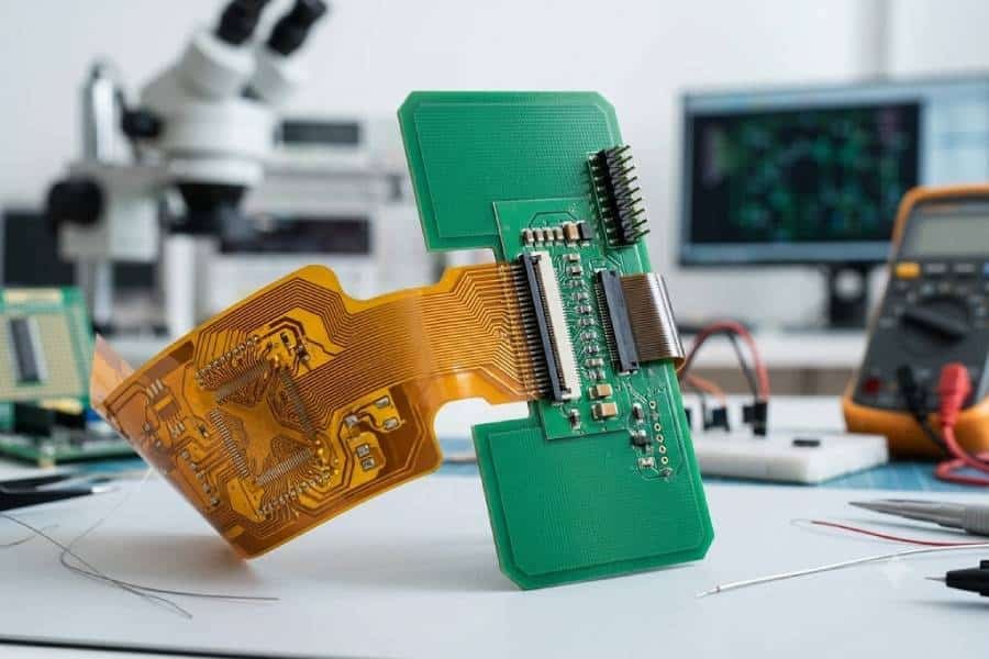
Introduction to Single-Sided Flexible PCB Design
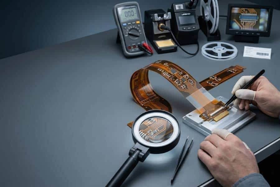
Single-sided flexible PCBs look simple compared to multilayer or rigid-flex designs, but their success still depends heavily on good mechanical and layout design decisions. Even with only one copper layer, the way you set the bend radius, route traces and place stiffeners will determine whether the flex circuit works reliably over its entire lifetime or starts to crack after a short period of use.
What is a single-sided flexible PCB in design terms
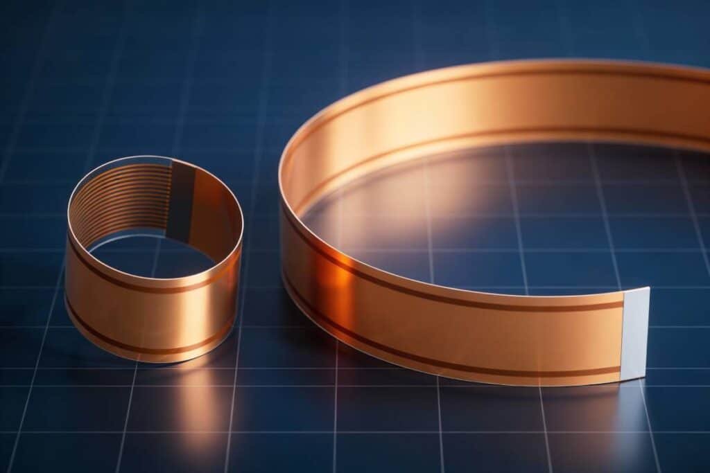
In design terms, a single-sided flexible PCB is a circuit built on a thin polyimide base film with copper on only one side, patterned to form traces and pads. The flexible substrate allows the circuit to bend, fold or twist so it can connect modules in three-dimensional space, replace wire harnesses and fit into tight mechanical envelopes. Because there is only one copper layer, designers must route all signals on that layer while still respecting mechanical constraints in the flex areas.
Why bending radius, trace routing and stiffeners matter most
Among all design parameters, bending radius, trace routing and stiffener design are the three that most directly affect the mechanical reliability of single-sided flex circuits. If the bend radius is too small for the flex thickness and copper type, the copper conductors and polyimide can experience excessive strain and eventually crack. Poorly planned trace routing, such as traces running in unfavorable directions or with sharp corners in bend areas, concentrates stress and accelerates fatigue. Stiffeners that are missing, oversized or placed in the wrong position can either leave critical joints unsupported or create hard edges that increase stress on the flex region.
Typical failure modes caused by poor flex design
When these mechanical aspects are not considered early in the design, several common failure modes tend to appear in single-sided flexible PCBs. The most typical issues include copper trace cracking along the bend line, pad lifting or delamination near stiffener edges and solder joint failure at components located in flexing areas. Designers may also see intermittent opens or high resistance due to micro‑cracks in traces, especially in dynamic flex applications where the circuit bends repeatedly. Many of these problems can be traced back to underestimated bend radius, unfavorable trace direction, lack of strain relief and insufficient collaboration with the flex PCB manufacturer in the early design stage.
Material Selection and Stackup for Single-Sided Flexible PCBs
The material system and stackup you choose for a single-sided flexible PCB have a direct impact on bendability, reliability, manufacturability and cost. Even though there is only one copper layer, the combination of polyimide base film, copper foil, adhesive and coverlay determines how well the flex circuit will survive bending and thermal cycling over its lifetime.
Core materials: polyimide base film and copper foil
Most single-sided flexible PCBs are built on a polyimide (PI) base film with a single layer of copper foil laminated on one side. Polyimide provides excellent heat resistance, mechanical strength and dimensional stability, which makes it the preferred material for medium to high‑reliability flexible circuits. The copper layer is typically either rolled annealed (RA) or electro‑deposited (ED); RA copper offers superior ductility and is better suited for dynamic flexing, while ED copper is more cost‑effective for static bend or limited-flex applications.
When designing a single-sided flex circuit, you need to balance polyimide thickness and copper thickness to achieve the required flexibility and mechanical robustness. Thinner PI and copper reduce the minimum bend radius and make the flex more compliant, but they also lower tear resistance and impact strength. For high‑cycle dynamic flex regions, designers often choose very thin PI (for example 12.5–25 μm) and thin copper, then rely on good mechanical design and local reinforcement to maintain strength where needed.
Coverlay and adhesive systems
Instead of liquid solder mask used on rigid PCBs, flexible circuits typically use coverlay films to protect the copper circuitry. A coverlay is usually composed of a polyimide film plus an adhesive layer (such as acrylic or epoxy) that is laminated over the copper under heat and pressure, with openings created mechanically or by laser to expose pads and soldering areas. Compared to flexible solder mask inks, coverlays provide better flexibility and durability in bending areas, so they are commonly used in the main flex regions of single-sided circuits.
Adhesive selection must consider operating temperature, flexibility and reliability requirements. For high‑temperature or high‑reliability applications, adhesiveless constructions or high‑temperature adhesive systems can offer smaller bend radii and improved thermal performance, at the cost of higher material and process expense. In cost‑sensitive consumer products with moderate bending demands, standard PI plus adhesive coverlay systems are often sufficient. During design, it is also important to match adhesive thickness to copper and coverlay thickness to prevent excessive squeeze‑out around openings that could interfere with soldering.
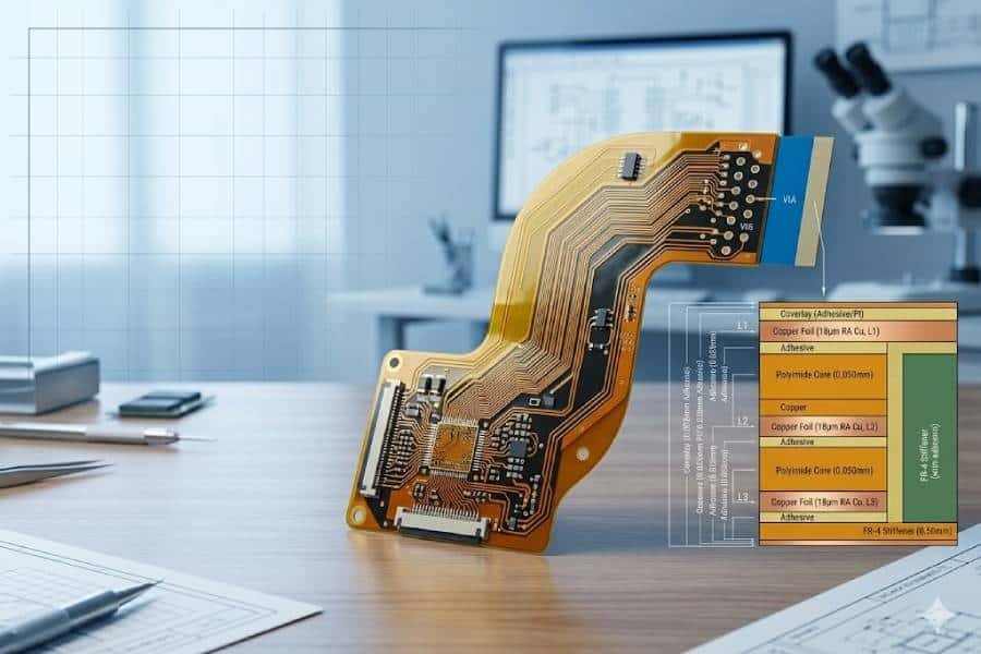
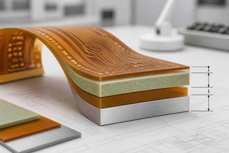
Typical single-sided flex stackup structures
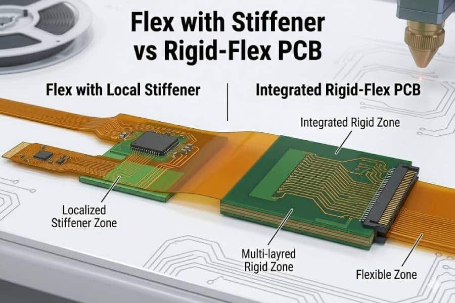
A typical single-sided flexible PCB stackup consists of the polyimide base film, copper foil, etched circuitry and a coverlay layer, with optional local stiffeners in selected areas. In its simplest form, the stackup can be represented as PI core + copper + circuit pattern + coverlay, where the main flexing regions remain thin and compliant. For areas that must support components or connectors, designers often add FR4, PI, aluminum or stainless‑steel stiffeners on one side to create locally rigid sections while keeping the rest of the circuit flexible.
Both adhesive‑based and adhesiveless constructions are used in single-sided flex designs. Adhesive‑based structures place an adhesive layer between PI and copper or between copper and coverlay, offering mature processes and lower cost; adhesiveless structures eliminate the adhesive layer, resulting in thinner, more flexible and more heat‑resistant circuits at a higher material and processing cost. In practice, it is best to work with your flex PCB manufacturer early to agree on a feasible single-sided flex stackup that meets electrical and mechanical requirements while keeping the structure as simple as possible to maximize yield and control cost.
If you like this style and depth, next I can write Chapter 3: Bending Radius Design Rules for Single-Sided Flexible PCBs, which will build directly on these material and stackup choices.
Bending Radius Design Rules for Single-Sided Flexible PCBs
Basic formula and recommended minimum bend radius
For single-sided flexible PCBs, the minimum bend radius is one of the most important mechanical design parameters. It defines how tightly the flex circuit can be bent without causing damage to the copper or the polyimide base film. A common way to estimate the minimum safe bend radius is to use the simple formula \(R = t \times N\), where \(R\) is the bend radius, \(t\) is the total thickness of the flex (including copper, PI and coverlay) and \(N\) is a factor that depends on the type of flex and how it will be used.
For single-layer flex PCBs, many design guides suggest using an \(N\) value between about 6 and 10 for general applications. That means the bend radius should be at least 6–10 times the total thickness of the flex. In more conservative or high‑reliability guidelines based on IPC and field experience, static flex regions may use factors around 6–10, while dynamic flex regions that bend frequently can require factors as high as 50–100, especially when thicker constructions or less ductile copper are used. As a practical starting point, you can treat 6–10× thickness as a minimum for static bends and use significantly larger radii for dynamic bends, then refine the numbers with your material data sheets and manufacturer recommendations.
Static vs dynamic flex design targets
Static flex regions are those that are bent into shape only once during assembly or installation and then remain in a fixed position during normal operation. In these areas, the flex circuit can typically tolerate smaller bend radii than in dynamic regions, because the mechanical stress is applied only a few times and not cycled repeatedly. For single-sided flex PCBs in static applications, a minimum bend radius of about 6–10 times the flex thickness is often considered acceptable when using suitable materials and proper layout.
Dynamic flex regions, by contrast, are subject to repeated bending during the product’s life, such as in hinges, moving sensor arms or wearable devices. In these cases, fatigue becomes a major concern, and the allowable strain must be much lower. Industry examples and application notes often recommend minimum bend radii on the order of 50–100 times the flex thickness for single-layer dynamic flex, especially when long service life and high bend cycle counts are required. Designers should treat these values as conservative guidelines and always validate critical dynamic flex designs through prototype testing under realistic operating conditions.
Design tips to reduce stress in bending areas
Regardless of the exact bend radius values you choose, there are several practical design techniques that can help reduce mechanical stress in the bending areas of single-sided flex circuits. First, try to keep the flex stackup as thin as reasonably possible in the bend region by using thinner PI, copper and coverlay, and by avoiding unnecessary stiffeners or reinforcement near the bend line. Second, avoid sudden changes in thickness at or very close to the bend, because step changes in stiffness tend to concentrate stress and can lead to cracking or delamination over time.
It is also helpful to distribute bends over a longer length rather than forcing the flex to bend sharply in a very short distance. Using smooth, gradual curves instead of tight, localized bends lowers the peak strain on individual traces and the dielectric. When possible, place the main bend in an area with relatively uniform copper distribution so that different parts of the cross-section share the mechanical load more evenly. Finally, always review bend regions together with your flex PCB manufacturer; they can often suggest small changes in thickness, materials or bend geometry that significantly improve reliability without major impact on the rest of the design.
Trace Routing Guidelines in Flex Areas
Good trace routing is essential to the mechanical reliability and electrical performance of single-sided flexible PCBs, especially in bend regions. The goal is to minimize stress on copper conductors while still meeting signal integrity, impedance and spacing requirements.
Trace direction vs bending direction
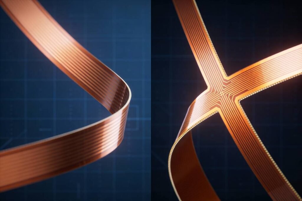
In flex areas, the direction of copper traces relative to the bend line has a major effect on how stress is distributed during bending. Whenever possible, route traces so that they cross the bend line perpendicular to the direction of bending, rather than running parallel to it. Perpendicular or moderately angled traces share the strain more evenly along their width, while long, parallel traces concentrate stress along their length and are more prone to cracking.
You should also avoid placing the highest‑priority or most sensitive traces exactly at the point of maximum curvature. If the mechanical design allows, shift critical traces slightly away from the tightest part of the bend, or increase the bend radius in regions where important signals must cross. For single-sided flex circuits that bend in multiple directions, use smooth routing transitions and avoid sudden changes in trace orientation that can create localized stress risers.
Trace width, spacing and copper distribution
Trace width in flex regions should not be driven only by current capacity or impedance; mechanical fatigue must also be considered. Using slightly wider traces in dynamic bending areas can reduce current density and mechanical stress, improving fatigue life, as long as the added copper does not make the region too stiff. Maintain adequate spacing between traces to prevent micro‑cracks from propagating directly from one conductor to the next in high‑stress zones.
Copper distribution across the flex cross‑section should be as uniform as practical. Large solid copper areas next to regions with almost no copper can create significant stiffness differences that concentrate bending stress at the boundaries. For single-sided flex PCBs, try to avoid very wide copper pours in the bend area; instead, use narrower conductors, cross‑hatched patterns or segmented shapes that provide the necessary electrical function without creating rigid “bars” across the flex.
Avoiding sharp corners and stress concentration
Sharp corners and abrupt geometry changes in copper traces act as stress concentrators and are a common cause of cracks in flex circuits. Replace 90‑degree corners with smooth arcs or chamfered bends, and avoid sudden transitions between very narrow and very wide sections of copper in or near the bend zone. Where traces enter or leave pads in flex regions, use fillets or teardrop shapes to provide a gradual transition and reduce the chance of cracking at the pad/trace interface.
It is also good practice to keep the number of trace crossovers and intersections to a minimum in bend areas to avoid complex local stress patterns. Group traces with similar mechanical requirements together and route them in parallel paths, instead of weaving them around each other. Finally, review bend regions in detail during design reviews and, if possible, simulate or prototype the flex in its bent state to confirm that no unexpected sharp angles or stress concentrators have been introduced.
Via, Pad and Component Placement in Single-Sided Flex Designs
Careful via, pad and component placement is critical for reliable single-sided flexible PCBs because all these rigid features sit on a bendable substrate. Good placement minimizes mechanical stress on copper and solder joints, reduces the chance of pad lifting and improves long-term flex performance.
Keeping vias and holes away from bend lines
Vias and plated holes behave like rigid points in an otherwise flexible structure and do not tolerate repeated bending well. Whenever possible, avoid placing vias directly in flex regions and keep them out of primary bend zones where the flex will experience the highest strain. As a rule of thumb, maintain a clearance distance between the bend line and any plated through holes, tooling holes or mechanical mounting holes, so that bending occurs only in areas of continuous copper and dielectric.
In single-sided flex designs, plated vias may be used less frequently, but any required holes for connectors, fasteners or mechanical alignment should still be located in flat, non‑bending sections. If you must route signals through a region near a bend, consider using gradual routing transitions and placing any necessary holes just outside the high‑strain area. Discuss critical hole locations with your flex manufacturer, who can advise on safe spacing from bend lines based on their material set and process capability.
Pad shapes, teardrops and anchoring in flex circuits
Pads in single-sided flexible PCBs are only bonded to the base film on one side, which makes them more susceptible to lifting and cracking than pads on rigid boards. To improve mechanical robustness, use filleted or rounded pad shapes instead of sharp rectangular corners, especially in flex regions. Adding teardrop connections between traces and pads provides a smooth transition in copper width and reduces stress concentration at the pad/trace junction.
Coverlay design also plays an important role in pad anchoring. Wherever possible, extend coverlay over part of the pad to create “anchor windows” that lock the pad more securely to the substrate while still leaving enough exposed copper for reliable soldering. Avoid very small annular rings and thin necks on pads in flex areas, and ensure that solder mask or coverlay clearances do not leave unsupported copper islands that can peel under mechanical or thermal stress.
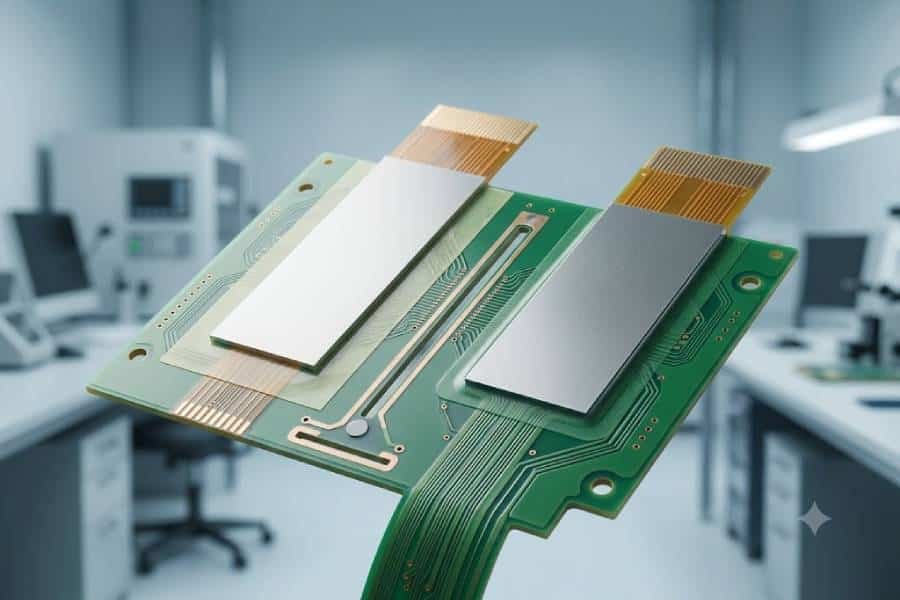
Placing components in reinforced, non-bending areas
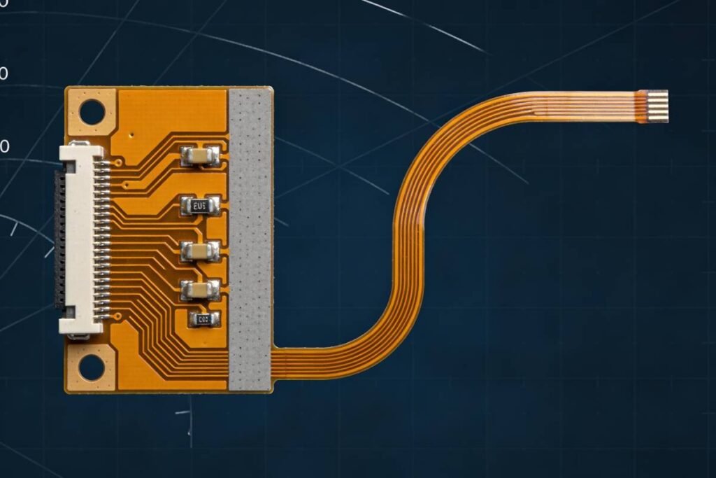
Components and connectors should always be located in areas that remain essentially flat during operation and are reinforced by stiffeners or the product housing. Do not place components in regions that are intended to flex, and keep a safety distance between the last row of components and the start of any bend zone so that solder joints are not exposed to repeated bending. This is especially important for heavier parts such as board‑to‑board connectors, switches and large capacitors, which can put significant mechanical load on their pads.
Under connector footprints and dense component clusters, use FR4, PI or metal stiffeners to create a locally rigid area that supports solder joints and helps maintain planarity during assembly. Design the stiffener so that its edge does not align exactly with the bend line; instead, leave a short transition region of unsupported flex between the stiffener edge and the start of the bend to avoid a hard hinge effect. Finally, review component placement in 3D relative to the enclosure and bending motion, making sure that parts do not collide with each other or with mechanical features as the flex circuit moves.
Using Stiffeners in Single-Sided Flexible PCBs
Stiffeners are an essential part of many single-sided flexible PCB designs because they create rigid areas where components and connectors can be mounted securely. When used correctly, they improve mechanical robustness and assembly yield without sacrificing the flexibility of the rest of the circuit.
When and why you need stiffeners
You typically need stiffeners wherever the flex PCB must behave like a small rigid board: under connectors, around component clusters, and in regions that will be gripped, inserted or screwed into an enclosure. Without stiffeners, solder joints in these areas can be stressed during handling, assembly and operation, leading to pad lifting or cracked joints over time. Stiffeners also help maintain coplanarity during SMT reflow, making it easier to achieve reliable solder fillets on small-pitch components.
In single-sided flex circuits, stiffeners are especially important under edge connectors, ZIF contacts and any area where external cables or harnesses will apply mechanical load. They can also be used to control the way the flex bends, guiding the bend to occur in safe regions rather than near sensitive components or pads. By selectively adding stiffeners, you can fine‑tune the mechanical behavior of the flex circuit to match the product’s assembly and usage conditions.
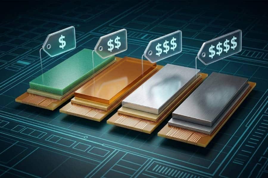
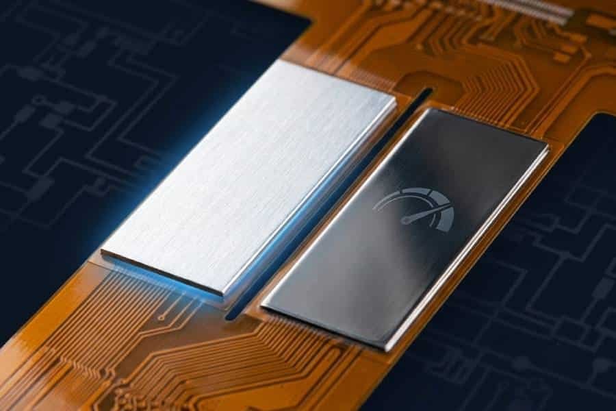
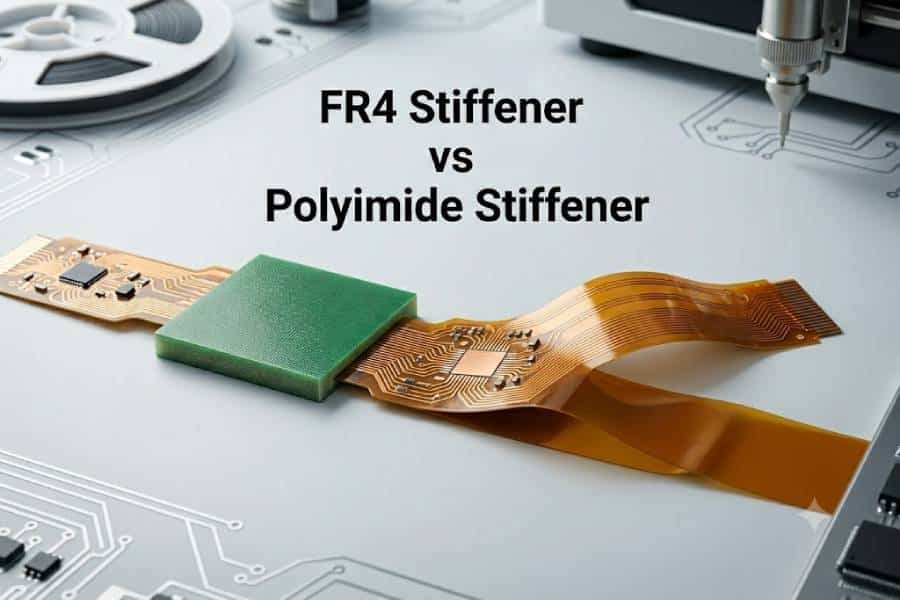
Common stiffener materials: FR4, PI, aluminum and stainless steel
The most common stiffener material for flexible PCBs is FR4, because it is inexpensive, easy to process and compatible with standard PCB fabrication and assembly equipment. FR4 stiffeners are widely used under connectors and component areas to provide rigidity and thickness, especially where the flex must match a card edge slot or mechanical guide. Polyimide stiffeners are thinner and more flexible than FR4, making them a good choice when you need some reinforcement without adding too much thickness or stiffness.
Metal stiffeners such as aluminum or stainless steel are used when higher mechanical strength or better heat spreading is required. Aluminum can help with thermal management under power components, while stainless steel offers very high stiffness for areas that must resist bending or pulling forces. When selecting a stiffener material, consider thickness, stiffness, thermal properties, weight and cost, as well as how the stiffener will interface with the enclosure or mounting hardware.
Stiffener placement rules around connectors and components
The placement of stiffeners relative to bend regions and component locations has a strong influence on stress distribution in the flex circuit. As a general rule, the stiffener should fully support the entire footprint of connectors and component groups, extending slightly beyond the outer rows of pads to provide a stable platform. At the same time, the stiffener edge should not terminate exactly at the bend line; leaving a short transition zone of unsupported flex between the stiffener edge and the start of the bend helps avoid a sharp hinge that concentrates stress.
Avoid placing stiffeners in areas intended to flex during normal operation, unless the goal is specifically to prevent bending in that region. In cable‑like sections, keep stiffeners out of the main flexing span and use them only at ends or branch points where the flex connects to rigid structures. Coordinate stiffener outlines with coverlay openings and component placement so that there are no unexpected overlaps or gaps that could interfere with soldering, assembly fixtures or enclosure features.
DFM and Collaboration with Your Flex PCB Manufacturer
Working closely with your flex PCB manufacturer is one of the most effective ways to avoid redesigns and unexpected reliability issues in single-sided flexible PCB projects. Design for manufacturability (DFM) reviews help align your mechanical and electrical requirements with real‑world process capabilities, materials and tolerances.
Typical DFM checks for single-sided flexible PCB designs
A thorough DFM review for single-sided flex circuits usually covers bend radius, stackup, copper distribution, coverlay design and stiffener locations. Manufacturers will verify that minimum bend radius values are realistic for the specified thickness and that bend regions do not include vias, sharp copper corners or severe thickness steps. They also check that trace widths, spacings and clearances meet their process limits and that panel utilization and routing strategies support good yield.
Coverlay opening sizes, positions and tolerances are another key DFM point, because misaligned openings can expose or cover pads incorrectly. Stiffener outlines and thicknesses are reviewed to ensure they can be bonded reliably and will not interfere with tooling or depanelization. For designs that include assembly, DFM checks may also cover component libraries, pad geometries, fiducials and test access to make sure the flex can be populated and tested using standard SMT processes.
Information you should provide to the flex PCB manufacturer
To get meaningful DFM feedback, you need to provide more than just Gerber files. At a minimum, share the intended stackup (including material types and thicknesses), the expected bend radii and locations, and whether each flex region is static or dynamic. Include any mechanical drawings or 3D models that show how the flex will be folded or installed in the final product, so the manufacturer can understand real‑world stress points.
If you plan to assemble components on the flex, provide a complete BOM, assembly drawings and any special requirements such as stiffener materials, adhesive types or preferred surface finishes. It is also helpful to indicate critical nets, controlled‑impedance lines and high‑current paths, so the manufacturer can confirm that routing, copper thickness and clearances are adequate. The more design intent you share, the easier it is for the flex supplier to suggest practical improvements instead of just flagging problems.
How early design review helps avoid redesign and failures
Engaging your flex PCB manufacturer early—before layout is finalized—can prevent many of the common issues that lead to late changes or field failures. Early DFM review can catch unrealistic bend radii, problematic stiffener locations, or coverlay designs that are difficult to manufacture, while there is still time to adjust the mechanical concept or routing. This reduces the risk of discovering cracked traces, delamination or assembly problems only after prototypes are built and tested.
Collaborating during the design phase also allows you to optimize cost and yield, for example by simplifying stackups, standardizing materials and improving panel utilization. Manufacturers can propose alternative constructions or process tweaks that maintain your performance targets while making the design easier to build consistently. In the long run, this kind of partnership shortens development cycles, improves reliability and helps ensure that single-sided flexible PCBs move smoothly from prototype to volume production.
Practical Design Checklist for Single-Sided Flex Circuits
A concise checklist helps ensure that key mechanical and layout rules for single-sided flexible PCBs are consistently applied before sending files for fabrication. You can use the following points as a final review list for bend radius, routing, vias, pads, components and stiffeners.
Quick checklist for bend radius and thickness
- – Confirm total flex thickness (PI + copper + coverlay) for each bend region and document it clearly in the stackup.
- – Verify that minimum bend radius is at least 6–10× thickness for static bends and significantly larger (for example 50–100×) for dynamic bends, unless validated by testing.
- – Check that there are no abrupt thickness steps or stiffener edges exactly at the bend line.
- – Ensure that critical bends are located in areas with consistent material construction and no unnecessary copper or mechanical features.
Quick checklist for trace routing and vias
- – In flex regions, route traces perpendicular or at a moderate angle to the bend direction rather than parallel to it.
- – Replace sharp 90° corners with smooth arcs or chamfered bends and avoid sudden changes in trace width in bend areas.
- – Review copper distribution to avoid large solid copper areas next to empty regions across the bend; use narrower traces or cross‑hatched patterns if needed.
- – Keep vias and plated holes out of primary bend zones and maintain a safe clearance between bend lines and any holes or mechanical fasteners.
Quick checklist for pads, components and stiffeners
- – Use rounded or filleted pad shapes and teardrop connections in flex regions to reduce stress at pad/trace interfaces.
- – Design coverlay openings and anchor features so that pads are mechanically supported and not left as isolated copper islands.
- – Place components and connectors only in non‑bending areas, supported by FR4, PI or metal stiffeners where necessary.
- – Ensure stiffeners fully support connector and component footprints and that their edges do not coincide with bend lines; leave a short transition zone of bare flex before the bend.
Using this checklist as part of your standard design review helps catch many common issues early and makes it easier for both your team and your flex PCB manufacturer to deliver reliable single-sided flex circuits on the first iteration.
Conclusion and Next Steps
Single-sided flexible PCBs offer a simple yet powerful way to route signals through tight, three‑dimensional spaces, but their success depends heavily on good mechanical and layout design. By choosing appropriate materials and stackups, respecting realistic bend radius limits and following sound routing, via and pad placement practices, designers can greatly reduce the risk of cracked traces, delamination and pad lifting in single-layer flex circuits.
Stiffeners, coverlay design and early collaboration with an experienced flex PCB manufacturer are equally important for building robust connector and component areas and ensuring manufacturability from prototype to volume production. Using a practical checklist before releasing your files for fabrication helps enforce these best practices and catch common issues early, saving both time and cost in development.
If you are working on a single-sided flexible PCB design and are unsure about bend radius, stackup, routing or stiffener choices, consider sharing your design files and mechanical requirements with your flex PCB supplier for a DFM review and design feedback. A short design consultation can often prevent multiple prototype spins and give your single-sided flex circuits a much better chance of meeting their reliability and lifetime goals in real-world applications.