Table of Contents
Why High Frequency PCB Design Needs Special Guidelines
Designing a low‑speed control board is very different from designing a high frequency PCB that must carry RF and multi‑gigabit signals with tight margins. At radio frequencies and high‑speed data rates, every detail—materials, stackup, trace geometry, grounding and even via placement—starts to behave as part of the signal path, not just as a mechanical support.
If traditional “draw a trace and it will probably work” layout habits are carried over into high frequency designs, the result is often unpredictable impedance, excessive loss, crosstalk and EMI problems that only show up during lab testing or, worse, in the field. To avoid this trial‑and‑error cycle, it is important to follow proven high frequency PCB design guidelines that align with what can actually be manufactured on RF materials and hybrid stackups. This article focuses on practical layout, stackup and routing practices for high frequency and RF PCBs, and highlights where it makes sense to involve an experienced high frequency PCB manufacturer early in the design flow.
Define the Design Context First
Before drawing any traces, effective high frequency PCB design starts with clearly understanding the electrical and manufacturing context of the project. Frequency range, bandwidth, interfaces, materials and fabrication limits all influence which layout guidelines matter most and how strict they need to be.
Clarify Frequency, Interfaces and Performance Targets
The first step is to define the operating frequency range and the types of signals that will run on the board, such as RF carriers, IF signals, clocks, SerDes links or other high‑speed interfaces. For each critical path, you should establish basic performance targets—acceptable insertion loss, return loss or reflection levels, jitter budgets and noise margins—so that stackup and routing decisions can be made with clear objectives rather than guesses. Mapping out the RF signal chain and key high‑speed links early also helps identify which nets require controlled impedance, extra spacing or stricter routing constraints.
Understand Material and Stackup Constraints from Manufacturing
In parallel, it is important to understand what high frequency materials and stackup options your PCB manufacturer can actually support, including available dielectric thicknesses, copper weights and typical impedance tolerances. Different shops may have different experience with PTFE‑based laminates, Rogers hydrocarbon/ceramic materials and hybrid RF + FR4 constructions, and these capabilities will influence which design rules are realistic for your project. A short early discussion with a high frequency PCB manufacturer to review candidate materials, layer counts and minimum trace/spacing can prevent situations where a beautifully simulated design turns out to be difficult or expensive to fabricate as drawn.
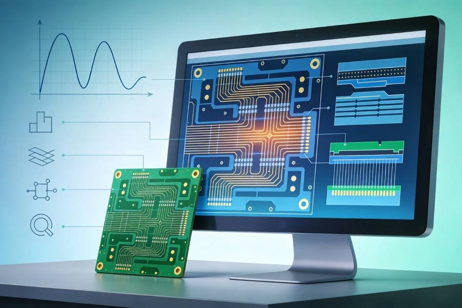
Stackup and Impedance Planning
A robust stackup is the foundation of any successful high frequency PCB design, because it determines the electromagnetic environment in which your traces operate. Choices about materials, layer order, dielectric thickness and copper weight all combine to set achievable impedance values, loss levels and isolation between different signal types.
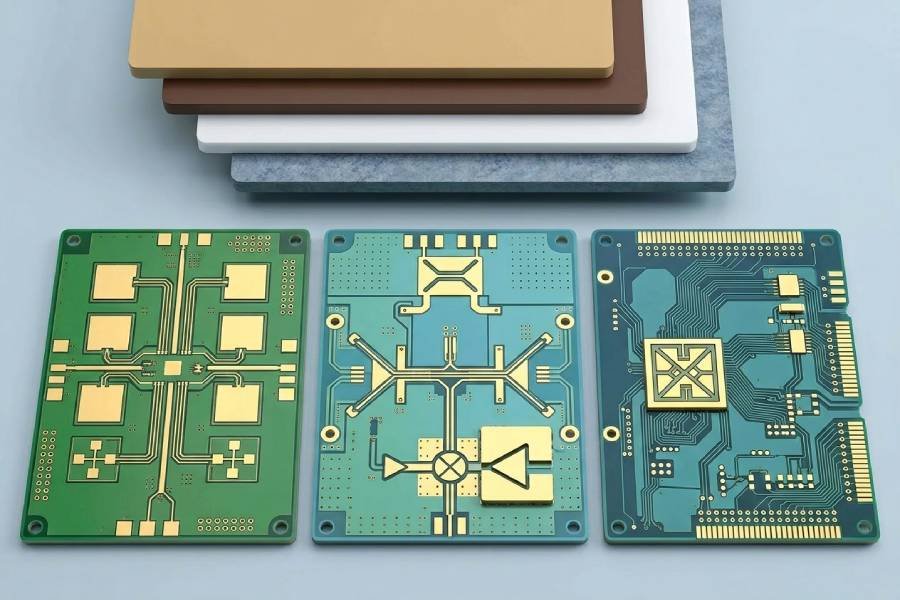
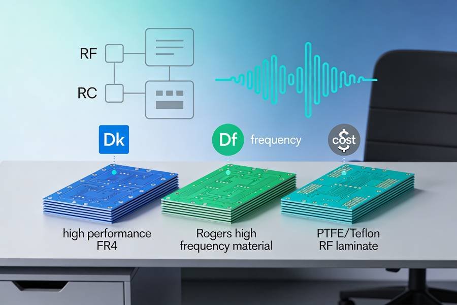
Choose Suitable High Frequency Materials
For RF and high‑speed designs, substrate selection should be driven by the required frequency range, loss budget, temperature stability and cost constraints. PTFE‑based laminates and Rogers hydrocarbon/ceramic materials offer low loss and well‑controlled dielectric constant for demanding RF paths, while high performance FR4 can be adequate for shorter high‑speed digital links or non‑critical sections of the board. In many cases, a hybrid stackup using RF materials for critical layers and FR4 for the rest provides a good balance between performance and manufacturability.
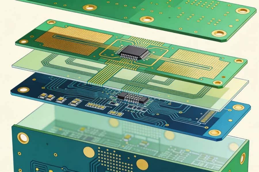
High Frequency Stackup Guidelines
A typical high frequency PCB will use at least four layers so that signal layers can be referenced to solid planes for controlled impedance and clean return paths. Common patterns include signal–ground–power–signal or signal–ground–ground–signal, where RF and high‑speed traces are routed either as microstrip on outer layers over a continuous ground plane or as stripline between two planes for better isolation. Keeping reference planes unbroken under critical lines and avoiding unnecessary splits or gaps in these planes is essential to maintain predictable impedance and minimize radiation.
Plan for Controlled Impedance Early
High frequency and high‑speed nets should be treated as controlled‑impedance transmission lines—typically 50 Ω single‑ended and 90–100 Ω differential, depending on the interface and standard. Impedance values are set by a combination of trace width, spacing, dielectric constant, dielectric thickness and copper thickness, so these parameters must be defined together rather than in isolation. Using impedance calculators or field‑solver tools with the exact material data and proposed stackup from your PCB manufacturer helps ensure that the line geometries you choose correspond to realistic, manufacturable structures.
Align Design Rules with Manufacturing Tolerances
Even the best impedance plan can fail if it ignores what the fabrication process can actually hold in production. Early in the design, you should confirm your manufacturer’s typical tolerances for trace width, dielectric thickness and copper thickness, as well as the impedance tolerance they can guarantee, and then incorporate these into your design margins. By aligning your stackup and impedance targets with realistic manufacturing capabilities, you reduce the risk that measured impedance and loss on real boards will deviate significantly from your simulations.
Component Placement and Layout Zoning
Thoughtful component placement and clear functional zoning make high frequency PCB routing much easier and help prevent many signal integrity and EMI problems before they appear. By grouping related circuits, keeping sensitive areas compact and planning signal flow early, you create a layout where high frequency guidelines can be applied consistently instead of being added as last‑minute fixes.
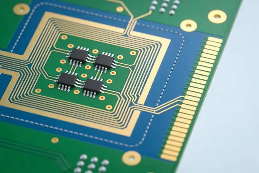
Functional Zoning of RF, Digital and Power Circuits
Thoughtful component placement and clear functional zoning make high frequency PCB routing much easier and help prevent many signal integrity and EMI problems before they appear. By grouping related circuits, keeping sensitive areas compact and planning signal flow early, you create a layout where high frequency guidelines can be applied consistently instead of being added as last‑minute fixes.
Place the RF Signal Chain Intentionally
A good starting point is to divide the PCB into logical zones: RF sections, high‑speed digital blocks, low‑speed control and power management. RF front‑ends, mixers, local oscillators and filters should be clustered together along the signal chain, away from noisy switching regulators, digital processors and fast I/O connectors. Clear boundaries between these zones, supported by appropriate ground and power arrangements, make it easier to control coupling and keep sensitive RF nodes away from high di/dt currents and fast digital edges.
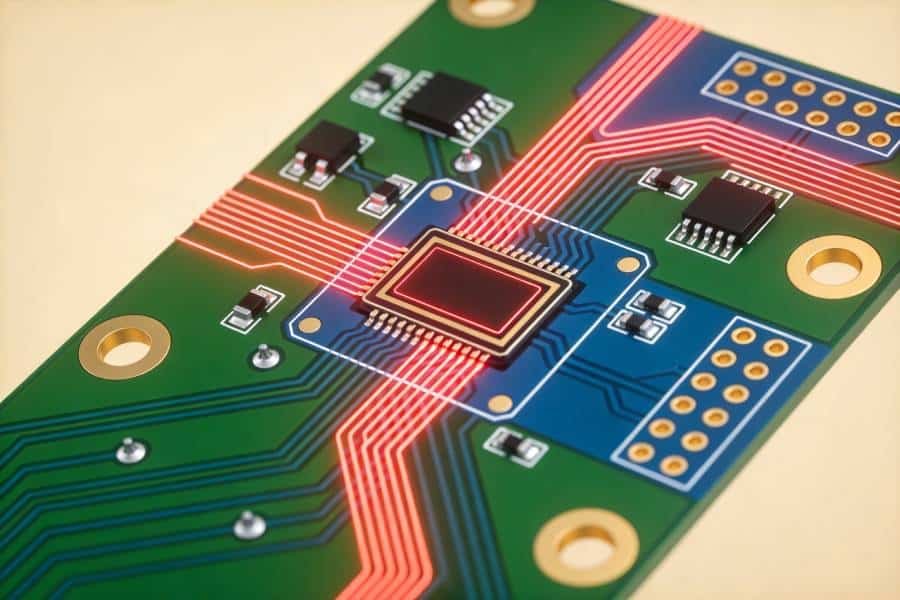
Keep High Frequency Interconnects Short and Direct
For both RF and high‑speed digital paths, long meandering routes increase loss, add delay and create more opportunities for coupling and radiation. Critical nets such as RF transmission lines, high‑speed clock traces and differential pairs should be kept as short and straight as practical, with minimal layer transitions and no unnecessary branches or stubs. When a layer change is unavoidable, placing stitching vias close to the transition helps maintain a tight return path and preserves the intended high frequency behavior of the interconnect.
Routing Guidelines for High Frequency PCBs
Once the stackup and placement are defined, routing determines whether your high frequency PCB will actually behave like the carefully planned transmission line system you intended. Good routing practice minimizes discontinuities, avoids unnecessary parasitics and keeps critical nets under control across all layers.
Treat Critical Nets as Transmission Lines
High frequency and high‑speed nets should always be routed with their characteristic impedance and return path in mind, not just as simple connections between pads. Use the controlled‑impedance geometries defined in your stackup—correct trace width, spacing to neighbors and continuous reference plane—to route RF lines, clocks and fast differential pairs, and avoid arbitrary neck‑downs or shape changes that would locally change impedance. Where connectors or component pads introduce unavoidable discontinuities, keep the affected region as short as possible and consider simple tuning structures or matching if measurements show problematic reflections.
Control Corners, Vias and Stubs
Sharp 90‑degree bends can slightly increase effective capacitance and cause impedance variation at high frequencies, so it is common practice to use 45‑degree bends or smooth arcs on critical RF and high‑speed lines. Each via adds inductance and a small impedance discontinuity, so minimize the number of layer transitions on sensitive nets and avoid leaving unused via stubs that act as resonant structures at certain frequencies. When layer changes are necessary, placing ground vias near signal vias and, where appropriate, using back‑drilling to remove long via stubs can significantly improve high frequency performance.
Use Layers Strategically and Separate Signal Types
High frequency PCBs benefit from assigning different signal types to specific layers, for example routing RF lines on one layer referenced to a solid ground plane and placing high‑speed digital traces on another, while keeping noisy switching signals and low‑speed control nets on separate layers. This separation reduces coupling between incompatible signals and simplifies stackup planning, because each layer can be optimized for its primary function. When routing between layers, try to maintain consistent reference planes and avoid crossing gaps or splits, which can force return currents to detour and create unintended loops.
Differential Pairs and Length Matching
Differential pairs used for high‑speed interfaces or certain RF structures require special attention to geometry and timing. Within each pair, keep the traces tightly coupled with consistent spacing to maintain the intended differential impedance, while providing adequate clearance to other signals to minimize common‑mode conversion and crosstalk. Length matching within a pair is important to control skew, and for multi‑lane buses or phased RF paths, additional inter‑pair matching may be required, but these adjustments should be implemented with gentle meanders that respect impedance rules rather than abrupt zig‑zags in congested areas.
Grounding and Return Path Control
Good grounding and controlled return paths are at the heart of reliable high frequency PCB design, because they determine how currents actually flow and how much noise, radiation and coupling your board will produce. Even with a well‑planned stackup and careful routing, poor ground implementation can quickly degrade RF performance and high‑speed signal integrity.
Use Solid Ground Planes Wherever Possible
High frequency designs work best with solid, continuous ground planes that provide a low‑impedance reference for signals across the entire operating frequency range. Large, uninterrupted ground planes directly under critical signal layers help maintain stable impedance, support clean return paths and reduce both emissions and susceptibility to external noise. Excessive use of split grounds or narrow ground “necks” under high frequency traces should be avoided, as they force return currents to take longer, more inductive paths.
Preserve Return Path Integrity at Layer Transitions
When a high frequency signal changes layers through a via, its return current must also find a way to transition between reference planes without creating a large loop. Adding stitching vias that connect ground planes near the signal via provides a short, low‑inductance path for the return current and helps maintain the transmission line behavior across the transition. Designers should avoid routing critical traces across gaps or slots in the reference plane, because this breaks the direct return path and can significantly increase radiation and crosstalk.
Grounding Strategies for RF and Digital Sections
RF and digital circuits often share the same PCB, but they do not always require physically separated ground planes; in many cases, a single well‑planned ground system works better than poorly executed splits. A common approach is to keep RF, high‑speed digital and noisy power sections physically separated on the board, while tying their grounds together at a low‑impedance point or using a solid common ground plane, so that return currents stay local to their signal paths. Where true ground partitioning is required—such as isolating sensitive analog front‑ends from high‑power switching stages—it should be done with a clear plan for how signals cross between regions and how their return paths are managed, often with controlled bridges or dedicated filtering.
Crosstalk, EMI/EMC and Power Integrity
Even with good stackup, routing and grounding, high frequency PCBs can still suffer from crosstalk, EMI/EMC issues and power integrity problems if coupling and supply noise are not controlled. Addressing these aspects early in the design reduces the risk of late‑stage failures during compliance testing or system integration.
Spacing Rules and Shielding Against Crosstalk
Crosstalk occurs when energy from an aggressor trace couples into a nearby victim, and its impact grows as edge rates and frequencies increase. Maintaining adequate spacing between sensitive nets—often two to three times the trace width for critical lines—and avoiding long parallel runs of aggressor/victim pairs on the same layer are simple but effective ways to reduce coupling. Where space is tight, grounded guard traces or routing critical nets as stripline between planes can provide additional isolation and help keep crosstalk within acceptable limits.
Layer‑to‑Layer Coupling Management
Crosstalk is not limited to traces on the same layer; fields from high frequency lines can couple through the dielectric to signals on adjacent layers if geometries are not planned carefully. A common guideline is to route signals orthogonally between neighboring layers—for example, horizontal on one layer and vertical on the next—to reduce broadside coupling. Placing solid reference planes between critical routing layers and avoiding stacking multiple high‑speed layers directly adjacent to each other without isolation also helps control inter‑layer coupling.
Decoupling Strategy and Power Distribution
Power integrity problems can manifest as jitter, phase noise or spurious emissions in high frequency circuits if supply rails are not properly decoupled and distributed. High frequency PCBs should use a hierarchical decoupling scheme, placing small, low‑ESL capacitors close to each IC power pin and complementing them with larger capacitors and, when appropriate, ferrite beads or filters to control noise over a wide frequency range. Designing power and ground planes to minimize loop areas and avoid narrow bottlenecks further reduces impedance peaks and helps keep supply noise from coupling into sensitive RF and high‑speed sections.
DFM and Working with a High Frequency PCB Manufacturer
Design for manufacturability (DFM) is especially important in high frequency PCB projects, because small mismatches between the design assumptions and real fabrication capabilities can lead to unexpected impedance shifts, increased loss or yield problems. Aligning your rules and simulations with what your manufacturer can repeatedly produce helps ensure that prototypes and volume builds behave as intended, not just in the CAD tool.
Design with Manufacturability in Mind
When setting minimum trace width, spacing, via sizes and impedance geometries, designers should use values that fall comfortably within the high frequency PCB manufacturer’s published capabilities rather than pushing absolute limits without a strong reason. Conservative design choices often improve yield, reduce cost and make impedance and loss more consistent from batch to batch. Documenting critical dimensions and tolerances clearly in fabrication notes also helps the shop prioritize what must be controlled most tightly.
Early Stackup and Impedance Review
Before finalizing the layout, it is good practice to share your proposed stackup, impedance requirements and key high frequency nets with your PCB manufacturer for review. The fabricator can validate whether the chosen material combination, dielectric thicknesses and trace geometries are realistic and may suggest adjustments that simplify production while still meeting electrical goals. This collaboration reduces the risk of multiple spins caused by impedance discrepancies or material availability issues that could have been caught earlier.
From Prototype to Production
Moving a high frequency PCB from prototype to production introduces additional considerations such as material sourcing, process repeatability and test coverage. Working with the same high frequency PCB manufacturer across both stages helps maintain consistent stackups, processes and performance, and allows lessons learned from prototypes to be folded directly into production builds. Ensuring that appropriate electrical testing and, when needed, impedance verification are included in the production test plan further increases confidence that every batch will meet the RF and high‑speed requirements of the design.
Summary
High frequency PCB design demands a more disciplined approach than low‑speed layouts, combining appropriate materials, carefully planned stackups, transmission‑line‑aware routing, solid grounding and attention to crosstalk, EMI and power integrity. By defining the design context up front and following practical guidelines for placement, routing and return path control, engineers can significantly improve the chances that first‑pass hardware meets RF and high‑speed performance goals.
Equally important is making sure that these design decisions are compatible with what a high frequency PCB manufacturer can reliably fabricate, from material choices and stackups to impedance tolerances and test strategies. Early collaboration with an experienced high frequency PCB fabrication partner helps turn theoretical guidelines into robust, repeatable hardware that performs consistently from prototype through volume production.
If you have not read it yet, you can review the basics in your “What Is High Frequency PCB?” article and then link readers from this design guide back to your High Frequency PCB manufacturing services page, inviting them to share their stackups and RFQ so you can support their next high frequency project from both the design and manufacturing side.